send me an e-mail , with snail mail addy
I'll send them as soon I manage solving proper fabrication of pcbs , with all mumbo jumbo needed for them to both look good and function good .
it will be soon .
problems with oscillation aren't because of pcb , but probably because of some unfortunate mix of output darlingtons and used caps characteristics ;
first - you can cure oscillation problems in 2 ways :
1. 10nF cap between B-E of darlingtons
2. decrease C14 and C14a to , say, 10uF
regarding your grounding scheme :
-put 10-15R NTC between signal gnd and safety gnd
-main signal gnd - considering that you're using same xformer(s) for both channels , must be taken from group of pads J4-J4a-J8-J8a ; make bridge of substantial gauge from these groups of pads between two Shuntys
for bridging signal gnd and upper gnd plane on Shunty pcbs use either JP2 or JP2A; that depends of actual physical layout in box , which one is better ; in some cases is best even to leave them unbridged .
edit : I remember extensive communication with guy who originally had problems with that set of pcbs ; grounding scheme was completely wrong , and it stayed wrong ....... in spite of all advices .
after I send you set of new pcbs , do not bother to ask for same advices again ; search and read ; everything is already covered .
Last edited:
Why am I seeing such horrible ripple at OS1 and OS1A with fuses in place.
There is no ripple at all if I remove the fuses and load the CRCRC circuits up to 200mA.
There is no ripple at all if I remove the fuses and load the CRCRC circuits up to 200mA.
send me an e-mail , with snail mail addy
I'll send them as soon I manage solving proper fabrication of pcbs , with all mumbo jumbo needed for them to both look good and function good .
it will be soon .
problems with oscillation aren't because of pcb , but probably because of some unfortunate mix of output darlingtons and used caps characteristics ;
first - you can cure oscillation problems in 2 ways :
1. 10nF cap between B-E of darlingtons
2. decrease C14 and C14a to , say, 10uF
regarding your grounding scheme :
-put 10-15R NTC between signal gnd and safety gnd
-main signal gnd - considering that you're using same xformer(s) for both channels , must be taken from group of pads J4-J4a-J8-J8a ; make bridge of substantial gauge from these groups of pads between two Shuntys
for bridging signal gnd and upper gnd plane on Shunty pcbs use either JP2 or JP2A; that depends of actual physical layout in box , which one is better ; in some cases is best even to leave them unbridged .
edit : I remember extensive communication with guy who originally had problems with that set of pcbs ; grounding scheme was completely wrong , and it stayed wrong ....... in spite of all advices .
after I send you set of new pcbs , do not bother to ask for same advices again ; search and read ; everything is already covered .
You infer "Used Caps". Everything is Brand New and highly specced.
I don't understand the circuitry well enough to start pulling components to see what is and isn't working.
It outputs +/- 36V OK.
.......
With the 470R load resistors, the current draw from both CRCRC supplies is about 145mA.
So nothing is shorted and drawing excessive current. Where is the 100Hz ripple coming from ?
hows that :
..... and I are are both seasoned electronic engineers as well as DIYers.
anyway :
You infer "Used Caps". Everything is Brand New and highly specced.
I didn't said that they're bad ; I said that combination of characteristics of caps and darlingtons sometimes is cause of oscillation ;
and I wrote how to cure that .
That might explain the 20MHz osillation but not the 100Hz ripple.
I'm not into RF electronics.
I'm not into RF electronics.
make grounding arrangement properly , put those caps at darlingtons , and ripple will be in projected ballpark .
Andy and I are are both seasoned electronic engineers as well as DIYers.
Well ...
If I were you,
I would try with modesty and simply following what Zm suggests
It would make things less confusing ...
Manu
That schematic looks quite comprehensive.
Considering only the top half.
C15, R23, C16, R24, C2 is your rCRCRC
You can read off the current flowing through the CRC by measuring the Vdrop on each of the 4r7 resistors.
Q1 is a follower configured as a regulator.
Measure Vds and Vgs to check it is doing as expected.
Q2 Q3 are a 2transistor CCS. The CCS current is ~VbeQ3 / R7.
Measure the Vbe and check the current flowing. It should match Ir23 = Ir24
Q11 is the Shunt regulator. Measure Vdrop R20. The output load current + Ir20 should be just slightly less than Ir23.
Q8 & Q9 are another 2transistorCCS. check the Vdrop of R17. Half of that current should pass through each half of the cascoded LTP. Measure Vdrop of R12.
However.
All your DC measurements are likely to have an error due to the circuit oscillation. The oscillation must be stopped first. Then proceed to post the measurements.
Well ...
If I were you,
I would try with modesty and simply following what Zm suggests
It would make things less confusing ...
Manu
Although I'm an electronic engineer, I'm a computer engineer, not an audio engineer.
Unfortunately my project doesn't have the room to stick additional components on the bopttom of the board.
I'll try these suggestions that have been offerred so far, however, I am finding it impossible to source the correct transformer.
RS do a 55-0-55V 120VA transformer, other than that, its buying a 30-0-30 and adding extra turns.
send me an e-mail , with snail mail addy
I'll send them as soon I manage solving proper fabrication of pcbs , with all mumbo jumbo needed for them to both look good and function good .
it will be soon .
problems with oscillation aren't because of pcb , but probably because of some unfortunate mix of output darlingtons and used caps characteristics ;
first - you can cure oscillation problems in 2 ways :
1. 10nF cap between B-E of darlingtons
2. decrease C14 and C14a to , say, 10uF
regarding your grounding scheme :
-put 10-15R NTC between signal gnd and safety gnd
-main signal gnd - considering that you're using same xformer(s) for both channels , must be taken from group of pads J4-J4a-J8-J8a ; make bridge of substantial gauge from these groups of pads between two Shuntys
for bridging signal gnd and upper gnd plane on Shunty pcbs use either JP2 or JP2A; that depends of actual physical layout in box , which one is better ; in some cases is best even to leave them unbridged .
edit : I remember extensive communication with guy who originally had problems with that set of pcbs ; grounding scheme was completely wrong , and it stayed wrong ....... in spite of all advices .
after I send you set of new pcbs , do not bother to ask for same advices again ; search and read ; everything is already covered .
I've done everything you suggest and there is absolutely no change in the symptoms.
I am at a loss on this one.
Attachments
Last edited:
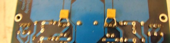
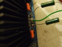
Ive only got JP2A connected. Not JP2. Ist it EITHER/OR or BOTH.
PLease bear in mind that I have removed this Shuntky from its case to try and figure out what is wrong.
PLease bear in mind that I have removed this Shuntky from its case to try and figure out what is wrong.
Attachments
Last edited:
try JP2 instead of JP2A
also - you can solder 2u2 (electrolytic is good enough ) across both C12 and C12A
also - you can solder 2u2 (electrolytic is good enough ) across both C12 and C12A
well ....... Gremlins on work ;
there is no way that pcbs are so trashed that voltage is ok , but oscillation is here - on all 4 legs .....
try any adequate TO-220 non-darlington transistors instead of darlingtons
to make that possible and adequate - solder additional 390R resistors across R12 and R12a
there is no way that pcbs are so trashed that voltage is ok , but oscillation is here - on all 4 legs .....
try any adequate TO-220 non-darlington transistors instead of darlingtons
to make that possible and adequate - solder additional 390R resistors across R12 and R12a
What I cant understand is that the current drawn through the two fuses is only about 146mA, with the 470R load resistors. Why is there such huge ripple (100mV) after the CRCRC filter. If you remove the fuses and measure the output of the CRCRC filter with a 500mA load it is CLEAN.
I reckon there is a broken track somewhere but how it is affecting both + and - supplies seems ODD.
what's difference between termocouple RF Ampermeter and usual DMM ....... ?
???????
Are you sure that is aimed at me.
- Home
- Amplifiers
- Pass Labs
- Pumpkin preamp - ordered by Steen , official making thread