My line of thought is "5mA at 12V, 10mA at 24V.. and if 10mA is too bright, add a series resistor"
I think I'll just add 100K resistors series resistors on all of the TPA control inputs and call it a day. Means shuffling a few parts to fit everything on the PCB.
No need to, just rewire the dip and change the two 75k pus.
You could add a CCS as the current sink ( if space permits) for the LED so that it is power supply independent.
Hi gmarsh,
I can't thank you and others here enough for what you are accomplishing in designing and building the Proper TAP amp board! It's a wonderful process to watch in action.
Please put me down for 1 completed and tested board. Will probably add 1 or 2 more later.
Cheers,
Rod
I can't thank you and others here enough for what you are accomplishing in designing and building the Proper TAP amp board! It's a wonderful process to watch in action.
Please put me down for 1 completed and tested board. Will probably add 1 or 2 more later.
Cheers,
Rod
That'll technically provide 100K+ series resistance with positive slew, technically negative slew would be still unacceptable... Though I s'pose connecting FAULTZ/SDZ violates that anyway and TI even suggests that.No need to, just rewire the dip and change the two 75k pus.
*shrug* I'll just change the pull-ups/switch as you're saying and call it a day.
Know one catch this one, i went over it a few times 🙂
my reasoning,
U2B: flip pins 5 & 6. In normal operation you want "sdz" high (pullup to PVCC) as it is active low.
At power up, pin 5 (+) is grounded, as C30 has no charge. pin 6 (-) is higher (your ref), so output pin 7 is off (open-collector bjt) or a high due to the pullup R11(75K). SDZ is active low, outputs hi-Z.
Once C30 charges up ( 1t=150ms) and crosses the pin 6 threshold, pin 7 goes low.
I looked at the TI DS, 8.2.1.1 & 8.2.1.2, to get it straight, I think 🙂 !!
SNOSBJ3E –NOVEMBER 1999–REVISED DECEMBER 2014
The Fairchild d/s is well, not the best, they are a second source after all, same goes for STMicro. This was originally a National part, looks like TI has improved the d/s in the last rev (since I looked again) but retained many of National original examples.
Look at fig 10.2, they even have a smt layout example, TI is a class act. but where is the schematic? 🙂
You could also add some hysteresis to the lm339 comparator, as in figures 24 & 25 of the tI d/s. This allows a clean switch, with no glitching, R's are cheap and optional. Also someone may use a mechanical switch for ext. shutdown "/OFF", so this will prevent switch bouncing.
🙂 LM339 always had me thinking because it is open collector, opposite to a comparator that is not o/c.
Your gain selection looks diff than the d/s. How do you get the 100K pull up?
From table 1. For master, 26dB you need 100K pull-up and 20K pull down, a 5/1 ratio, 150/30.1=
okay i see now what you have done, by including slave operation too, a few calculation to make.
Part suggestions,
1) suggest to use the snubbers, R5-8, I used a 250mW (0805) snubber R
660-SG73P2ATTD10R0F
2) make a dual footprint for input coupling caps,c31,32,34,35, so that one can use 10uF smt caps ( a 10uF film cap is rather BIG, for 32dB gain, input Z is 9Kohm) f=1/2piRC =1.77hz, with a 2.2uF you will get 8Hz
"If a flat bass response is required down to 20 Hz the recommended cut-off frequency is a tenth of that, 2 Hz."
810-C3225X7R1E106M (10uF/25V/1210)
Oh, ya, put a rev or change date on your schematic, so we can keep track 🙂 Aren't design reviews fun? 🙂
Cheers
Rick
Last edited:
Most discussion way over my head, but put me down for two completed boards please. Thank you for your time and effort.
Didn't get much accomplished tonight as one of my dogs had surgery earlier, but got in about an hour of work.
Changes:
- Added shunt C's to the output snubbers
- moved terminal blocks slightly outwards to make more room (goddamn this board is tight now, but I'm determined not to exceed 5x10cm)
- added 1210 caps in the same footprints as the input film caps (thanks rsavas for the suggestion!)
- added PBTL straps to left input, in same location as film caps (don't populate caps, populate zero ohm resistors instead or just bridge with a blob of solder)
- Added ferrites at TPA INx pins at doctormord's suggestion.
- changed ESD protectors on audio inputs to SD36C's, added same to LED and standby inputs.
Layout:

Schematic (excuse the huge PNG)

Changes:
- Added shunt C's to the output snubbers
- moved terminal blocks slightly outwards to make more room (goddamn this board is tight now, but I'm determined not to exceed 5x10cm)
- added 1210 caps in the same footprints as the input film caps (thanks rsavas for the suggestion!)
- added PBTL straps to left input, in same location as film caps (don't populate caps, populate zero ohm resistors instead or just bridge with a blob of solder)
- Added ferrites at TPA INx pins at doctormord's suggestion.
- changed ESD protectors on audio inputs to SD36C's, added same to LED and standby inputs.
Layout:
Schematic (excuse the huge PNG)
Last edited:
rsavas: LM393 +/- are correct in the schematic to the best of my understanding - if +>- then output is open circuit, if +<- then output is grounded. If this wasn't the case then half the examples in the 393 datasheet wouldn't work - note the 'comparator with hysteresis' example in this one:
http://www.onsemi.com/pub_link/Collateral/LM393-D.PDF
Looking at adding hysteresis now, gonna mess around in LTspice for a while.
http://www.onsemi.com/pub_link/Collateral/LM393-D.PDF
Looking at adding hysteresis now, gonna mess around in LTspice for a while.
Same here. Way over my head but would like to have two completely finished boards. Plan to put them into a multi-channel amp for its chasis and power supply.
Hope your dog faired well and a speedy recovery hopefully.
You're not on a schedule for this project are you? I remember Gant charts, MS project.
Who is on the critical path?, hope it is not me 🙂 Once we (h/w guys, chips/pcb) got the s/w guys a working proto, we had some breathing room. s/w guys always padded the schedules 🙂
Cheers
You're not on a schedule for this project are you? I remember Gant charts, MS project.
Who is on the critical path?, hope it is not me 🙂 Once we (h/w guys, chips/pcb) got the s/w guys a working proto, we had some breathing room. s/w guys always padded the schedules 🙂
Cheers
The first 90% of a project uses 90% of the schedule.
The other 10% of the project uses the other 90% of the schedule.
🙂
Looks good so far.
The other 10% of the project uses the other 90% of the schedule.
🙂
Looks good so far.
He's doing ok. Had a benign fatty tumor in his rear left leg that had to be cut out, they got most of it out but had to leave a bit in place around his sciatic (sp?) nerve, fingers crossed it won't grow back. Right now he's still half drugged out on anesthesia, and has an ugly incision stitched up on the back of his leg that'll take a couple weeks to fully heal up.Hope your dog faired well and a speedy recovery hopefully.
You're not on a schedule for this project are you? I remember Gant charts, MS project.
Who is on the critical path?, hope it is not me 🙂 Once we (h/w guys, chips/pcb) got the s/w guys a working proto, we had some breathing room. s/w guys always padded the schedules 🙂
Cheers
Glad I'm getting lots of interest in this project though, profits from assembling boards will be paying off the vet bill. Part of me wants to draw a little Charlie doodle and poke it on the board somewhere. Here he is:

Critical path is me. To do:
- Get hardware design finished. I've decided to spend the extra buck and put down a trimmer pot for PLIMIT. Hopefully that's it for hardware changes...
- Get BOM finalized, figure out what parts get ordered from what distributor.
- Price boxes, static bags, etc. and come up with a good shipping estimate.
- Start group buy, probably gonna kick it off this weekend and take orders for 2 weeks. Get bed of nails tester design done during that time.
- Order parts/PCBs for amps and tester.
- Twiddle thumbs until everything comes in, I'll probably use Seeed Studio or dirtypcbs for the PCBs, so it'll take a few days to fab and a week or two to arrive.
- When everything arrives, build testers and start banging out PCBs.
Good to hear about your dog. Nice pic btw
Fig 12 in TI LM339 d/s is bugging me now, it is contary to
Got to like the new disclaimer,
that is good use of your hard efforts.Glad I'm getting lots of interest in this project though, profits from assembling boards will be paying off the vet bill.
Fig 12 in TI LM339 d/s is bugging me now, it is contary to
Or am I all messed up?7.4 Device Functional Modes
A basic comparator circuit is used for converting analog signals to a digital output. The output is HIGH when the voltage on the non-inverting (+IN) input is greater than the inverting (-IN) input. The output is LOW when the voltage on the noninverting (+IN) input is less than the inverting (-IN) input. The inverting input (-IN) is also commonly referred to as the "reference" or "VREF" input.
Got to like the new disclaimer,
Application and Implementation
NOTE
Information in the following applications sections is not part of the TI component specification, and TI does not warrant its accuracy or completeness. TI’s customers are responsible for determining suitability of components for their purposes. Customers should validate and test their design implementation to confirm system functionality.
I know datasheet tells me to put gnd for negative SE inputs at source, but that always seems to increase noise here, so I connect negative to ampboard gnd. Would r37 and r43 reduce/prevent that noise? (btw same added noise here with inputtransformers)
Do these 4 resistors affect inputimpedance and attenuation, I mostly use passive log pots, do they look like the loglaw resistors too added to linear pots? I don't remember clearly.
Do these 4 resistors affect inputimpedance and attenuation, I mostly use passive log pots, do they look like the loglaw resistors too added to linear pots? I don't remember clearly.
I know datasheet tells me to put gnd for negative SE inputs at source, but that always seems to increase noise here, so I connect negative to ampboard gnd.
...
Are you using shielded twisted pair wiring to the source?
Good to hear about your dog. Nice pic btw
that is good use of your hard efforts.
Fig 12 in TI LM339 d/s is bugging me now, it is contary to
Or am I all messed up?
Got to like the new disclaimer,
Well, it should work like it said.
7.4 Device Functional Modes
A basic comparator circuit is used for converting analog signals to a digital output. The output is HIGH when the voltage on the non-inverting (+IN) input is greater than the inverting (-IN) input. The output is LOW when the voltage on the noninverting (+IN) input is less than the inverting (-IN) input. The inverting input (-IN) is also commonly referred to as the "reference" or "VREF" input.
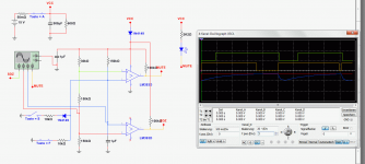
Verified earlier but did once more to make sure. 🙂
Attachments
Are you using shielded twisted pair wiring to the source?
both with standard cinch cable (coaxial) and twisted pair with additional earth wire and shield, several sources, <1 meter. not just dugs but all other (pbtl) I tried, and looking at dug pics I think it isn't just me, it seems several pics show ampboard-gnd connected to negative input, for your ampboards it just is visable easily🙂
- Status
- Not open for further replies.
- Home
- Amplifiers
- Class D
- "Proper" TDA3116 PCB