Somebody's stolen the GND connections...
Oh no! I'll take a look!
Last edited:
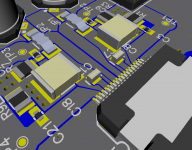
I'd recommend to stitch around all the top output traces for minimum impedance. 0.3mm vias would do. (From my own experience)
Thanks DrMord. I spotted a few designs installing 3.3n to 10n 0605 caps right before the speaker terminals for EMI reduction. Are these preferable?
Attachments
Last edited:
If they can handle the full output voltage swing in this size + safety margin? Yes, i have than too. Btw. Does all your inputs are ESD safe?
Hi,
I see that this design progresses steadily and with the support of kowlegeable persons.
I'm pretty sure it will be a very interesting project when looking for full digital amp!
Kind regards,
JMF
I see that this design progresses steadily and with the support of kowlegeable persons.
I'm pretty sure it will be a very interesting project when looking for full digital amp!
Kind regards,
JMF
The 100n would be better as small case X7R caps, far better for local bypass in the smallest package you can handle. The Panasonic are rather large and have to much parasitic inductance, look at the inductance curves on the data sheet. A lossy X7R in a small (low inductance case) is what is required for low value and local to power pins decoupling, being lossy limits anti resonance peaks, being low inductance means they work at a higher frequency, this is what is required for high dI/dT switching and instantaneous current supply.
Marce,
It's BOM time and costing.
Looking back on your comments some time ago.
For local bypass I spotted these
TDK 0.1uf 50v reversed 1632 -- $0.43
https://product.tdk.com/info/en/documents/chara_sheet/C1632X7R1H104M070AC.pdf
http://www.mouser.com/ProductDetail/TDK/C1632X7R1H104M070AC/
Murata 0.1uf 50v reversed 1632 -- $0.51
http://www.mouser.com/ds/2/281/c02e-2905.pdf
http://www.mouser.com/ProductDetail/Murata-Electronics/LLL31MR71H104MA01L/
AVX 0.1uf 50v reversed 1632 -- $1.21
http://www.mouser.com/ds/2/40/licc-776614.pdf
http://www.mouser.com/ProductDetail/AVX/06125C104KAT2A/
Shame they're not 63V or 100V.
Benefit here is that I can close up the supply stage a few mm. However, closer could mean warmer = lower capacitance with X7R.
As the AN points out ...
"Please, note that an inductance due to a PCB track of only ~15mm submitted to a current variation of ~3A in 15nsec, generates spikes in the range of 3V"
Last edited:
Hi,
I see that this design progresses steadily and with the support of kowlegeable persons.
I'm pretty sure it will be a very interesting project when looking for full digital amp!
Kind regards,
JMF
Thanks. We're getting there.
I've been messing around with the MSI motherboard mentioned earlier with the UPL and learning how to use that for testing. The 7 channel PRE out card is interesting. The DAE-3 is working as a PWM DAC --> 3 state bugger --> JRC 4580 dual op amps.
The TDK chart seems too hold capacitance quite well between 20c and 60 deg c. I'll see if I can make that fit nicely and bunch up a little more.
For bypass ST recommend a 50v 1u Tantalum or X7R.
1u 50v 1210 Tant with low ESR (300mOhm)
http://www.mouser.com/ProductDetail/AVX/TCJB105M050R0300/
2.2u 63v 1210 Tant with low ESR (200mOhm)
http://www.mouser.com/ProductDetail/AVX/TCJC225M063R0200/
Kemet have a new 1u 2220 film cap with 1e-2 @ 100Khz
http://www.mouser.com/ProductDetail/Kemet/LDEDD4100KA0N00/
http://www.mouser.com/ds/2/212/KEM_F3078_LDE-462598.pdf
The next caps to specify are the
3 x 100n bypass caps for the internal regulators and logic gates
1 x 100n bypass for the 3.3v incoming signals
All 50v 10% MLC X7R or otherwise.
Previous ref designs have also had an additional 100n between GND-SUB and VccSign.
3 x 100n bypass caps for the internal regulators and logic gates
1 x 100n bypass for the 3.3v incoming signals
All 50v 10% MLC X7R or otherwise.
Previous ref designs have also had an additional 100n between GND-SUB and VccSign.
Tantalum is made from conflict minerals, please don't use it.
https://en.m.wikipedia.org/wiki/Conflict_resource
Btw. 1632 caps ain't small and these TDK don't do much current:
https://product.tdk.com/info/en/documents/chara_sheet/C1632X7R1H104M070AC.pdf
https://en.m.wikipedia.org/wiki/Conflict_resource
Btw. 1632 caps ain't small and these TDK don't do much current:
https://product.tdk.com/info/en/documents/chara_sheet/C1632X7R1H104M070AC.pdf
Last edited:
It's a shame AVX isn't providing any useful plots for their products. (except some frequency plots) 🙁
Last edited:
Indeed. Going to all the effort to make a reversed part and not really displaying the merits. Not good. One of these days I will try with several differnt caps and measure the real world differences with the UPL.
What does the jumper and the increase in PSU traces add, the huge Wima size adds too. I would take a look at TI evm's for openloop amps and see how they filter/provide power to those ampchips, ripple gets directly into output TI showed.
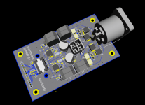
I made a start on the DSP board last night.
So far we have
LM340MP -> 5v
LP5097-3.3 for analogue section
LP5097-3.3 for digital section
LP5097-1.8 for clock and PLL
LM117-1.8 for core
GXO-3306G/B 24.576MHz 1.8v clock source
2 x SPDIF in -> Newawa transformer -> dsp
1 x dsp -> Newawa transfomer -> SPDIF
ADC input header
1 stereo pair but worth having around ~ THD-81/SNR95. Looking at OPAMP options so this can be used if required.
Outputs
Headers exposing 12 channels of PWM output mapped to 18 pins. Can be driven as PWM DACs - 8 or 16mA drive.
Install simple passive filters to deliver 1Vrms line level or opamps for more intersting outputs.
~ 104 db single ended
~ 114 db differential
I/O
i2s/DSD/HDA/TDM and USB for programming.
Attachments
Last edited:
What does the jumper and the increase in PSU traces add, the huge Wima size adds too. I would take a look at TI evm's for openloop amps and see how they filter/provide power to those ampchips, ripple gets directly into output TI showed.
The jumper saves having to route power through vias to the gnd plane. I thought it would be a neater solution. I am rethinking choices of components now.
Several EVMs and designs I've found from TI/NXP/IRS tend to use a single 2.2uF X7R for bypass with the bulk cap.
This particular part seems popular.
http://www.mouser.co.uk/ProductDetail/Murata-Electronics/GRM31CR71H225KA88L/
Attachments
Last edited:
MLCC is not only temperature dependent, but voltage dependent too. 100 nF will be only about 50 nF at rated voltage (but this depends on the exact type very much). Bigger ones can be better. I found good ones in 1206 only. (X7R can be strongly voltage dependent too, not only Y5V!)
And 100 nF is not neccessarily enough. With the parasitic inductance of the electrolytic cap it can resonate and causes an impedance peak. 10 nH 100 nF gives 5 MHz. X=0.3 ohm. If ESR is lower than this, then the resulting impedance at resonance will be even higher. But if ESR is higher, then it is a problem alone.
So to avoid this problem I use as high capacitance close to pins as possible. In the latest design 100 nF directly next to pins, but on the other side 4*2u2 connected through 5 parallel vias. This gives much smaller impedance at resonance. And ESR of polimer electrolitic is selected to damp this resonance to Q=1.
- Status
- Not open for further replies.
- Home
- Amplifiers
- Class D
- Project Moshulu : a journey into class D