Thanks Pafi for sharing.
Here's the low ESR PCR1V331MCL1GS 330uF I was considering.
http://www.mouser.com/ds/2/293/e-pcr-880064.pdf
tan 0.08
esr 16mOhm
3.9A ripple at 100Khz
Perhaps a little more evil than friend.
Here's the low ESR PCR1V331MCL1GS 330uF I was considering.
http://www.mouser.com/ds/2/293/e-pcr-880064.pdf
tan 0.08
esr 16mOhm
3.9A ripple at 100Khz
Perhaps a little more evil than friend.
Last edited:
Thanks Pafi. I like your thinking. Thanks for sharing.
I had also considered the following.
supply -> 330uF -> 10uF -> 1uF -> load
0603 50v 1uF X7R 10%
http://www.mouser.com/ProductDetail/Taiyo-Yuden/UMK107AB7105KA-T/
0603 50v 100nF X7R 10%
http://www.mouser.com/ProductDetail/Taiyo-Yuden/UMJ107BB7104KAHT/
3626 50v 10uF X7R 10% - low ESL & tan 0.05
https://product.tdk.com/info/en/documents/chara_sheet/CKG32KX7S1H106K335AH.pdf
1210 50v 10uF X7R - tan 0.1
http://www.mouser.com/ProductDetail/Taiyo-Yuden/UMK325AB7106KM-T/
4 x 0805 2u2
http://www.mouser.com/ProductDetail/Taiyo-Yuden/UMK212BB7225KG-T/
Last edited:
2u2 100V 1210 or 1206, Murata probably shows sims for all things you like to know, inductance 1210 a little lower than 1206 I recall
If the 16mohm polymer ers isn't too far from ceramic esr peaking might be ok ???
If the 16mohm polymer ers isn't too far from ceramic esr peaking might be ok ???
hello SPGU,
Very impressive! I like your project and i'm very interested.
My own porject is to use a minishark and feed by I2s 3*FDA (triamp)
I will follow this tread very closely. good luck
Very impressive! I like your project and i'm very interested.
My own porject is to use a minishark and feed by I2s 3*FDA (triamp)
I will follow this tread very closely. good luck
I've ordered V0.1 of my STA516BE stereo amp. I would like to build it and measure it. I placed some extra exposed pads for testing/adding additional comps if required. I'll provide an update in a week or so on that.
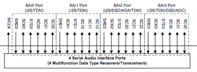
Next on the agenda is the DSP board. We have 4 digital I/O ports available.
Do I need to worry too much about digital isolation? A bit tricky when they are transceiver ports. I might consider isolation for SAI2 Port ( possible HDA connection to a PC motherboard codec).
Next on the agenda is the DSP board. We have 4 digital I/O ports available.
Do I need to worry too much about digital isolation? A bit tricky when they are transceiver ports. I might consider isolation for SAI2 Port ( possible HDA connection to a PC motherboard codec).
Attachments
Last edited:
2u2 100V 1210 or 1206, Murata probably shows sims for all things you like to know, inductance 1210 a little lower than 1206 I recall
If the 16mohm polymer ers isn't too far from ceramic esr peaking might be ok ???
Yes, Murata and also Samsung have online database showing all the parameters needed including DC bias effects. Worth to check them.
ESR of polimer cap should equal to Xc, not ESR of MLCC. 16 mohm is somewhat lower than optimal. I use 2 in series.
Thanks again. The esr of the PCR Nichicon is a little low. I'll do the math and make sure we're good.
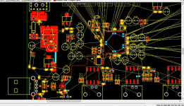
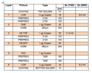
Making some progress with the DSP board. Laying out with this 6 layer stack up.
Layer 1 - Signal 1 (Low Speed Signal)
Layer 2 - GND
Layer 3 - Signal 2 (High Speed Signal)
Layer 4 - Signal 3 (High Speed Signal)
Layer 5 - VCC
Layer 6 - Signal 2 (Low Speed Signal)
I've been considering the PWM output routing. Any tips here? There are 9 pairs of PWM_HI/PWM_LO - 3.3v CMOS.
Would it be prudent to route as impedance matched differential pairs with
PWM_HI to layer 2 with PWM_LO directly beneath on layer 3?
Attachments
DrM, here's the proposed stack up. This is one of several standard 6 layers at my printers.
Attachments
Last edited:
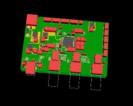
Sneak peak pic so far.
The three RCA conns ( 43-028 ) on the bottom edge are the 2 x SPDIF in / 1 x SPDIF out. They are from Canford in the UK but I've seen them elsewhere under other brands.
DELUXE RCA (PHONO) PANEL SOCKET PCB mounting, black
Just behind them are the Newava S37211 digital transformers. I look forward to a loop through test with the UPL to assess the DSP.
Across the top edge are the i2s, TDM, HDA and DSD inputs. On the right we have the 18 PWM out pins along with pins for amplifier feedback (protection etc).
On the bottom left is the USB port for programming the DSP.
I have been looking again at power for the PWMvdd pins. These pins form an internal ring for the PWM engine / PWM drive controller.
Perhaps these would benefit from a very low noise supply in the audio band and also excellent PSSR past 1Mhz.
LT3042 - 200mA LDO
PSRR: 105 dB at 10 kHz , 89 dB at 1MHz
Noise: 0.8µVRMS - 10 Hz to 100 kHz
It appears that the digital I/O also shares the power ring with the ppm section. Hmm.
Attachments
Last edited:
PWM signal is not that sensitive for amplitude noise. It has a susceptibility of fsw*(tr+tf). Channel separation is more important. I regularly use very noisy devices (like fast optocouplers) for transmitting PWM without significant problem. The key is fast transition. (And some feedback. I can't live without it. 🙂 )
Waouh !
What would be your idea about the clocking scheme for the I2S inputs ? Master or Slave or both options?
Do you consider some clock circuit on the DSP board?
By the way, I have been working on porting fractional delay code from Charlie Laub on a Nucleo Stm32F746 board, and I don't succeed yet to execute it fast enough for real time...
Kind regards,
JMF
JMF,
Clocking could be either, set by firmware/UI.
I'm using a Golledge low noise 1.8v 24.576 crystal 25ppm. Similar to NDK.
http://www.golledge.com/pdf/products/osc_sm/gxo3306.pdf
Clock available on XTALO @ 1.8v
MCLK output is also available at 3.3v, drive strength 8mA or 16mA.
Clocking could be either, set by firmware/UI.
I'm using a Golledge low noise 1.8v 24.576 crystal 25ppm. Similar to NDK.
http://www.golledge.com/pdf/products/osc_sm/gxo3306.pdf
Clock available on XTALO @ 1.8v
MCLK output is also available at 3.3v, drive strength 8mA or 16mA.
- Status
- Not open for further replies.
- Home
- Amplifiers
- Class D
- Project Moshulu : a journey into class D