release candidate
Hi All,
did some more changes to the layout. Thermal area is now 15x20mm both sides (gonna calculate if it will be enough), track length and vias have been reduced and in and output are now on the same side of the board. Overall board size is 50mm x 45mm.
If there are no significant bugs i'll probably order some boards for prototyping. PM me if you want to join 😉
regards, Daniel
Attachments

Hi,
The power suppl paths still look long, especially the positive, that crosses the complete PCB. I' suggest to place small ceramics close to R1 and R4, or/and Placing R2 where R24 is, resp C3 where the out connector is. Then I'd place all connectors as a single con at the lower rim of the PCB.
Con could be simple 90 degrees angled RM2.54 types.
A upright mounting on a Motherboard will then allow for most efficient cooling as You could glue a heatsink on each side of the PCB over both thermals.
You may want to add resistor pads to replace the potis with fixed values.
Especially for P2, as it may be that even fully open it may still not be enough for maximum modulation symmetry.
The thermal cross of the gnd-Pads of the troughhole Caps look quite thick. This may make soldering harder, as they conduct heat to the large gnd area.
Is there a special reason to go throughhole with those caps?
If the boards were to be manufactured in a groupbuy, this could cost extra against SMD caps.
There' s no Zobel at the output. The circuit seems to work stable without, but it'd add safety against capacitive loading. Fastron's L-0805-AS inductance, wound on on ceramic bodies may be appropriate.
C8, the modulation cap looks rather small sized. Is it a 220nF film cap?
Turn C5 by 90 degrees to allow for space for a cooling fin for J1/T3/T4.
jauu
Calvin
Last edited:
Hallo,
I also did a hand-drawn layout to self etch, for the schematic in #87 (left).
Actually, it is the first time that I used more than one SMD component, so I am not really sure if pad sizes and spacings are appropriate, but I think it should be ok.
The size for a single channel is about 35mm x 59mm. I used SMD parts for resistors and small caps, the transistors, trimpot and decoupling caps are through hole. The SMD parts themselves are relatively big: they are 1210 size, but again, this is the first time for me using SMD stuff. I had to use one wire link for the signal input to the FETs.
The voltage supplies are laid out for the use with Salas regs, so there is a sense connection for V+ and V-. There are three connections to the main power ground necessary. One from the signal star ground, and two from the decoupling caps. Any opinions about the grounding scheme are appreciated. Obviously, a ground plane is not possible, and an on-board main ground point would have been just as long-winded as the wire-based solution I chose, but with less flexibility.
As far as I l know, Salas regs do not really like additional low ESR decoupling caps, so there is the possibillity to connect V+ and V- with a serial R (Rser) or add an artificial ESR to a film decoupling cap (Rsh), or use a high ESR decoupling cap with the R-positions jumpered.
To be honest, I don´t know what should work best here, but at least I would have the options..
I added an input filter used by J. Gerhard and the output filter with a through-hole inductor. What kind of inductor is used best here?
Heatsinking for the four-FET-cluster can be done for example with IC-mini heatsinks or to220 heatsinks, glued from the top. I would have liked the FETs to be flat-to-flat oriented for more flexible glueing by a T-profile (or similiar) but now the are round-to-flat oriented, so thermal coupling should be done from above. (Or by the special mini heatsinks from XEN-audio, #10 works perfectly for this arrangement of FETs).
For the output transistors, I have to think of an appropriate way to cool, probably some glued IC heatsink.
Here ar the drawings, hand drawn with vectorworks. Any comments are appreciated:
Regards
Florian
An externally hosted image should be here but it was not working when we last tested it.
Do you have a current overall schematic of the complete unit?
I guess you are referring to the "complete unit" with buffer and gain stage discussed earlier?
Not my used "complete unit" which is post 87, left, with additional 500R/200p lowpass at the input.
Hi,
The power suppl paths still look long, especially the positive, that crosses the complete PCB. I' suggest to place small ceramics close to R1 and R4, or/and Placing R2 where R24 is, resp C3 where the out connector is. Then I'd place all connectors as a single con at the lower rim of the PCB.
Con could be simple 90 degrees angled RM2.54 types.
A upright mounting on a Motherboard will then allow for most efficient cooling as You could glue a heatsink on each side of the PCB over both thermals.
You may want to add resistor pads to replace the potis with fixed values.
Especially for P2, as it may be that even fully open it may still not be enough for maximum modulation symmetry.
The thermal cross of the gnd-Pads of the troughhole Caps look quite thick. This may make soldering harder, as they conduct heat to the large gnd area.
Is there a special reason to go throughhole with those caps?
If the boards were to be manufactured in a groupbuy, this could cost extra against SMD caps.
There' s no Zobel at the output. The circuit seems to work stable without, but it'd add safety against capacitive loading. Fastron's L-0805-AS inductance, wound on on ceramic bodies may be appropriate.
C8, the modulation cap looks rather small sized. Is it a 220nF film cap?
Turn C5 by 90 degrees to allow for space for a cooling fin for J1/T3/T4.
jauu
Calvin
Hey Calvin,
thank you very much for your comments!
I really like the idea of being able to mount/connect the buffer to a mainboard. Would be a nice building block for several applications like preamp (e.g. with muses), DAC (output buffer e.g. after JG Filter) or Phonopre.
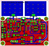
Thus I made another layout (forget about the release candidate from previous post, now v0.4, some are left until v1.0 😱) with the connector at the lower rim. Obviously the power lines have to be quite long and thus I added local decoupling caps (SMD 1206 case, e.g. 10µF MLCC) close to R1 and R4. I also played arround with moving R2/R3 outside but didn't manage to get real benefits.
I originally used through hole elcaps as they seem to be easier to hand solder and I like the mandatory vias they provide to ground plane. However I changed to SMD for the latest layout as a test/alternative. Used quite a lot of vias for the GND connection, might be too much wrt heat conduction (hard to hand solder). Any comments are welcome.
Good that you mentioned the modulation cap C8. Somehow I had 220pF (instead of 220nF) in my mind when choosing the case
 I replaced it with Panasonic ECHU PPS Film cap which is quite big.
Area of J1/T3/T4 is now free of other components thus placing a cooling fin should be possible (if it turns out to be necessary/worth, afaik Joachim didn't have much problems).
Will the added output inductor (Fastron 0805AS 1500nH) need a parallel R or is the DC resistance (2.3Ohm) sufficient? Should be no problem to add one...
I added resitor pads for P2. For P1 the pads of the pot could be used.
Best regards, Daniel
Attachments
Hi,
looks neat to me. 😉
Adding the C3/C8 also has the advantage that You don´t need low ESR caps for C4/C7 (in fact lowESR would be anti- beneficial here).
Those would definitely be easier to solder if they are Throughholes as the SMD-C or -D casings are really fiddly to solder.
Choosing SMD here is rather a Q for a professional production run. But one could also think of staying throughhole here and let the enduser solder them in .... kind of keeping the DIY-idea at least a bit and allowing nerds to tweak to death with boutique Caps. ;-)
The Panasonic PPS is a very good choice for C8.
The heat power loss of the CFP² places lower stress on the JFET-Duals and the average 67mW for T3/T4 stays well within the limits of the SOT23 casings, but will lead to noticeable tempereature rise. And less heat is always beneficial and a common thermal surrounding too.
A small IC-cooler for DIP14/16 like the V 5619A available from Reichelt at 0,32€ will suffice.
The CFP² seems stable against capacitive loading, so even the slightly lossy inductance is not necessarily needed. It´ll make the buffer probabely idiot-cap-proof. I assume no additional parallel R is required, but adding the pads for a 0805-R is easy and doesn´t harm.
Reichelt doesn´t list the 1500nH Fastron but most other values from 2200nH to 2.2µH, for example the L-0805AS 1,0µ at 0,15€.
Jst a last minor Q. Is it possible to cover the thermal vias on the cooling areas with solder resist also? The laquer would function as insulation layer if a common heat sink were glued over both areas like the V 5619E.
jauu
Calvin

Hi,
now fastly Approaching the finishing line 😉
What's now missing is a mechanical fixature.
I'd suggest to increase the height and width of the PCB slightly to allow for the montage of a guide rail. Only fixation via the connector may not be sufficiently stable, the more so the more mass, i.e cooling fins, are located at the top end of the PCB. A single guide rail may solve any mechanical issues.
See for example Fischer Elektronik FS 85 50 or MSVL 50
Add 3-4mm on the right side of the PCB for the guide and some mm in height if You use a connector like Fischer's MK51 or SL3 series. And don't forget the height required by the mating connector 😉
Fischer of course is known for their wide range of cooling fins. Maybe one can group buy cooling fins and connectors from them directly.
jauu
Calvin
Hi,
as addition.
Cooling fins from Fischer for the power transistors could be:
SK470 11.8*8*50mm (28k/W)
SK469 13.5*15.24*50mm (10.5K/W)
SK516 51 TO 218 21*10*51mm (25.2K/W)
or multiples of
ICK 14 16 B (V5619A) 19*4.8*6mm (50K/W)
ICK SMD B 10 or B13 19*4.8*10mm or13mm (35K/W or 29K/W)
3 to 5pcs. of the ICK14 16 B will probabely economically best.
The 3 CFP-transistor casings will dissipate 200mW and the power transistors 300mW to 600mW (depending on Bias current).
This should suffice to keep the temperature rise below ~25°C above ambient.
jauu
Calvin
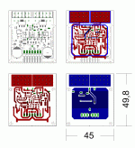
Hi all,
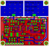
added some width and a slot for the MSVL 50 guide. Also added some height for angled pin headers. Using 8.5mm female connectors the slot should fit to the corresponding lock pin of the MSVL 50 guide. Overall board size now is 50mm width and 47mm height.
I set up a BOM for all electronic parts at mouser. Components will sum up to about 20€ incl. the LSK389C (not available at mouser) per board. The trimmer P1 and P2 make up quite a big part of the cost (9.50€). Not included are the pin headers, the cooling devices and the guide and the PCB itself.
Best regards, Daniel
Attachments
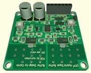
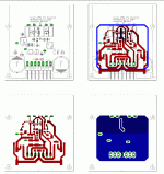
Hi,
had to do a own layout anyway ;-)
45 x 49.8mm format, with fins for card guide mounting, optional mounting holes, 3-5 cooling fins, improved power supply paths, separated supply- and analog-GND, 6 Test pads included.
I´ve already layouted a CFP I-V converter in same size format and style.
Probabely the symmetrizer/Gain-stage and the Calvin-Buffer will follow.
jauu
Calvin
Attachments
Last edited:
OK, if you plan to do a group buy i'll stop my efforts and take the easy route 😉
Watje 🙂 (Fluff-bol)
Hi,
I need to first check if a DIY approval will be granted.
And I haven´t yet organized nor taken part in a groupbuy and I won´t like a situation where I could be at an financial risk or I had to make prepaiments.
You know, I feel quite comfortable beeing the "eye in the sky", every now and then shooting some friendly fire at some innocent brave DIY souls*lol*
jauu
Calvin
Watje 🙂 (Fluff-bol)
Yep 😀
I like Calvins design (as far as I can see, the resolution is terrible 😉) so why should I do another one (I have so many other projects waiting...)?
@Joachim: we should not scare anyone doing groupbuys 😉 They are a very important part of this community and they give a lot of feedback to the designer. I've done some small GBs (the Buffer will probably not be small 😱) and yes, it's a hell lot of work especially if you include parts.
But if everyone just organizes one, we will have enough for the next years. So, come on Calvin, do it 😀
Do you know that several parts for my inductor buffer and the Paradise pre-regulator are sold out for at least half a year because such a big amount was ordered ?
Before you make a group buy on the Calvin buffer i would make sure that enough parts are available.
Before you make a group buy on the Calvin buffer i would make sure that enough parts are available.
- Home
- Source & Line
- Analog Line Level
- Preamp-Buffers - simple idea