the Zener and the diode are swapped.
The Zener will pass current and have a Vf of ~600mV when installed in that direction.
The diode will not pass current and as a result the protection fails.
The Zener will pass current and have a Vf of ~600mV when installed in that direction.
The diode will not pass current and as a result the protection fails.
This is the only other way I can think it must be. Is this correct ?
If this is correct then I can see why they are connected this way. Due to the NPN and PNP drivers ? Sorry I did not Read your post comprehensively. The last schemetic must then be correct. 🙂
If this is correct then I can see why they are connected this way. Due to the NPN and PNP drivers ? Sorry I did not Read your post comprehensively. The last schemetic must then be correct. 🙂
Attachments
Last edited:
Both pairs have to be connected in a way, as shown on the left picture at the bottom (in parallel with R22).

But they are both in series with each other. I cannot understand how it can make a difference. Well that why I asked you guy's. Thanks a lot all ! 🙂
Right, there's no difference as soon as you keep the right polarity of the devices.
Diode - anode is more positive, zener - cathode is more positive.
Diode - anode is more positive, zener - cathode is more positive.

the Zener passes current in BOTH directions.
The Diode passes current in ONE direction, It blocks current in the other direction.
The purpose of the gate protection is to prevent a high voltage pulse on the gate exceeding the permissible Vgs max specified in the datasheet.
The total voltage drop of Zener Vr and diode Vf must add up to less than Vgs max.
If Vgs max is specified as 15Vgs
then choosing a Zener of 14V and adding a diode with a Vf of ~700mVf gives a total of 14.7V.
This is getting a bit close to Vgs max.
Usually better to leave at least 2V to 3V spare below Vgs max. 12V Zener + 700mV diode is about as high as you want to go for a 15Vgs max.
Now go and look at the mosFET curves. What current will flow through the mosFET at your lowest Vds, if you limit the Vgs to a volt less than your Protection voltage? ( we leave a little bit lower than the nominal (Vr + Vf) because the diodes will start to turn on at lower than nominal voltage). You don't want the protection starting to turn on with a valid signal.
If the ID curves show you have lot's of spare current capability, you can choose a lower Vr for the Zener. You sometimes see a designer choosing 6.8V Zener, because they have looked at the Id curve and decided they don't need the protection voltage to be any higher than 6.8+0.7 - 1V
Thanks for the explanation Andrew. The datasheet states VGS max as +-20V. The rest of the sheet is a bit confusing as it gives different VGS values such as the gate threshold voltage of 4V, so which to use ? 😕
Oh I see it , the lowes current is 250uA at a minimum of 4V.
Oh I see it , the lowes current is 250uA at a minimum of 4V.
Last edited:
look at the whole range of Id vs Vgs.Thanks for the explanation Andrew. The datasheet states VGS max as +-20V. The rest of the sheet is a bit confusing as it gives different VGS values such as the gate threshold voltage of 4V, so which to use ? 😕
Oh I see it , the lowes current is 250uA at a minimum of 4V.
Some will be >10Apk How much current does your load demand?
That will determine the maximum Vgs that you need to apply for a valid signal. Your protection must allow the valid signal to pass.
Last edited:
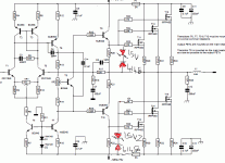
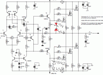
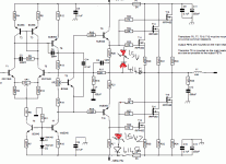
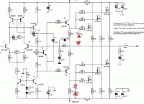
Andrew, is this that you are talking about ?
 The attachment does not seem to open.
Id@tc =25degC continuous drain current VGS@10V 30A
Id@tc=100degC Continuous drain current VGS@ 10V 21A.
So if VGS is 10V then I need a 9.3V zener with the diode ?
Id@tc =25degC continuous drain current VGS@10V 30A
Id@tc=100degC Continuous drain current VGS@ 10V 21A.
So if VGS is 10V then I need a 9.3V zener with the diode ?
Last edited:
I can't see it either.
But it looks like you have the diag.
If you NEED 21Apk to pass to the load when Vds is at your chosen lowest value, then what Vgs is required to get that Id?
Now add on a margin to ensure that Vgs does not get clipped too early.
That protection value is where you would set your Vr + Vf.
Check what side of the source resistor that your protection attaches to.
Some go to output rail and these must take account of the volts drop across Rs.
Andrew, the Vd over the source resistors are about 10mv. If you add that in it will be 9.4 V zener plus the 700ma of the diode ? 9.4+.700=10.1V.
- Home
- Amplifiers
- Solid State
- Power amp under development