IRFP460A vs IRFP450's
Cheers,
Shawn.
In harmony with John, the IRFP460 looks very suitable. MOSFET losses are directly related to the RDS(on) parameter. Lower Rds(on) means lower power loss and higher efficiency. If you set your amp up similarly to the others on the thread, I doubt you would be able to hear the difference. We're talking about the audio frequency range of the human ear which is nothing to the frequency these devices are designed to switch at. An improvement that would be seen in test equipment. Spending the time and money to DIY your own power amp, you should do what makes YOU happy and you control the budget😉PM650 said:Quick question here: would the IRFP460A's be worth the extra expense, over the 450's? Or are they even suitable in the first place?
Cheers,
Shawn.
I have a quickie question I never considered before about paralleled output devices.
If I understand correctly paralleled output devices Ciss's are added (as normal for paralleled capacitors). So for example using three output devices that have a Ciss of 3000pf would mean the driver stage sees 9000pf.
Then should it follow with Rds as well using ohms law where if Rds is 0.24 for the three output devices the driver stage sees 0.24/3 = 0.08 ohms?
I am aware that this will not change the losses associate with Rds for the output devices, but maybe this paralleled Rds has impact on output stage as some designs have a limit how much total capacitance the driver stage can be loaded with.
Comments, thoughts?
Regards,
John L. Males
Willowdale, Ontario
Canada
27 June 2006 02:33
You might ask yourself what the Rds value is of the fancy Japanese lateral Mosfets, or Semelabs new oldies.
Hint, it's a whole lot more than common Rds values of vertical mosfets. Only way in the TO3 mosfet output stage days to keep output voltage level flat across the impedance range was to use plenty in parallel.
The effect of the total input capacitance depends on the kind of output stage. I've also thought for too long that Ciss was the main parameter to reckon with to achieve decent slewrate numbers of mosfet output stages. Slewrate and Vpp determine the rise time, the rise time determines the bandwidth the output stage is capable of. Fortunately i read that guys like Erno Borbely made the same mistake, almost as long as me.
For EF stages it's the Crss value that is of importance. As that one is often only 1/10th of the Ciss number the driver current capability also reduces by the same factor.
Seems that plenty designers in the 80s and early 90s didn't really know the ins and outs of Mosfets, just copy-catted eachother.
I've communicated with 4 amplifier designers in those days who used the Ciss routine, funny no ? In those years i regarded all of them as genuine Gurus.
Hi,
no.
Rds is the effective resistance for the drain to source when the FET is turned on (Rds Resistance-drain-source)
The driver NEVER sees the output condition with a FET.
The FET behaves as if it had infinite input resistance (at the gate) in parallel with the capacitances (9nF).
The driver sees this capacitance and the others as a decreasing load as the frequency rises.
If you limit your amp to about 50kHz and work out the reactance of 9nF it gives you some idea of the kind of currents the driver has to pass at high frequency.
As far as the speaker is concerned it sees the source impedance of the three FETs in parallel and will respond by behaving a little differently from being fed by only one FET. Speaker Q varies with source impedance.
jacco,
Your last posting was very interesting regarding Ciss vs Crss. EF if I understand means Emitter Follower? If so can someone advise me if quasi's n-channel amp here is an EF design? My hunch is yes as I have noticed comments in this thread in past to effect that the design seems to be tollerant of high Ciss and perhpes it is moe due to the related Crss?
As to slew rate, I find one needs to take a few different device specifications and perform a set of calculations to determine the device effective slew rate of device. It is interesting how varied the slew rate abilities of the various mosfet devices is.
Andrew,
Thanks for the insight on Rds. I was not sure and suspected Rds has no bearing on paralled devices simply as nobody has ever noted this point in the question I raised on Rds and parallel devices. Still I am a curious sort and thought I better ask and not assume my lack of reading on the question either way.
Regards,
John L. Males
Willowdale, Ontario
Canada
27 June 2006 07:30
Hello,
A few really quickie questions here. An I do not need to know the theory or such to these what are they called questions:
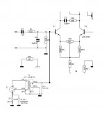
1) Is T2/T3 called current mirror pair?
2) Are T6/T7 called the predriver?
3) What is T4 called?
4) Are T9/T10 called drivers?
5) Has anyone any experience using the KSE340/350 instead of the MJE340/350 in general, or if by some chance with quasi's amp here?
All I need to know is what these are called of my attempts to suggest what I think they are called are incorrect. It is just for the parts list I am creating to figure out what parts I have, how many and what else I need to still purchase. For the transistors I have their purpose listed in case I need to explain to someone what the part is or how relates to part I am looking for. That is all.
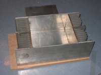
BTW, Shawn, very nice case. I look forward to how you squeeze everything in their considering the size of the toroid which I am very familar with it's size.
Regards,
John L. Males
Willowdale, Ontario
Canada
28 June 2006 11:23
28 June 2006 11:26 Typo correction
A few really quickie questions here. An I do not need to know the theory or such to these what are they called questions:
1) Is T2/T3 called current mirror pair?
2) Are T6/T7 called the predriver?
3) What is T4 called?
4) Are T9/T10 called drivers?
5) Has anyone any experience using the KSE340/350 instead of the MJE340/350 in general, or if by some chance with quasi's amp here?
All I need to know is what these are called of my attempts to suggest what I think they are called are incorrect. It is just for the parts list I am creating to figure out what parts I have, how many and what else I need to still purchase. For the transistors I have their purpose listed in case I need to explain to someone what the part is or how relates to part I am looking for. That is all.
BTW, Shawn, very nice case. I look forward to how you squeeze everything in their considering the size of the toroid which I am very familar with it's size.
Regards,
John L. Males
Willowdale, Ontario
Canada
28 June 2006 11:23
28 June 2006 11:26 Typo correction
Hi Key,
based on schematic from page 20.
T2 & T3 form a current mirror.
T4 & T7 in combination with D1 & D2 are constant current sources.
T6 is the VAS (voltage amplifer stage - some call this the current to voltage amp).
T9 & T10 are the drivers.
based on schematic from page 20.
T2 & T3 form a current mirror.
T4 & T7 in combination with D1 & D2 are constant current sources.
T6 is the VAS (voltage amplifer stage - some call this the current to voltage amp).
T9 & T10 are the drivers.
Hi Andrew,
Thanks for your reply. Clearly I was wrong even on some of the transistors functional pairings, but that is ok. At least I know now.
Regards,
John L. Males
Willowdale, Ontario
Canada
29 June 2006 06:32
Thanks for your reply. Clearly I was wrong even on some of the transistors functional pairings, but that is ok. At least I know now.
Regards,
John L. Males
Willowdale, Ontario
Canada
29 June 2006 06:32
keypunch said:
It is interesting how varied the slew rate abilities of the various mosfet devices is.
Slew rate is not intrinsically a property of a MOSFET - in theory, you could turn a MOSFET on or off as fast as you can add or remove charge to it's gate - the rest is only subject to transit time limitations, which for structures that small don't come into play until you get into the GHz region. The limitation to the ries and fall of the drain current arise due to finite currents charging and discharging the gate capacitance. Secondary, all currents pass through wires, which exhibit inductance, therfore a tendency to opose current changes. This is where the real limits are.
Thanks for the insight on Rds. I was not sure and suspected Rds has no bearing on paralled devices simply as nobody has ever noted this point in the question I raised on Rds and parallel devices.
Paralleling devices does indeed parallel Rds - two equal devices in parallel, together have half the Rds. The point made above is that Rds has no bearing in an amplifier application as it refers to the MOSFET working as a switch. For amplification purposes, we normally view a MOSFET as a transconductance device, where a certain Vgs makes the MOSFET pass a constant current, regardless of Vds. In reality, this is true only over a certain value of Vds - below which, the MOSFET behaves similar to a resistor. The Rds is calculated from the slope of the Id versus Vgs graph below this voltage, also known as the saturation voltage. In amplifiers, this condition would exist only when they are attempting to drive load impedances close to Rds. For the grand majority of amplifiers. The actual Rds will be a moot point as in general your MOSFET will be subjected to far greater problems at these conditions, like currents and power dissipations well over rated maximums. Here is an example: old style lateral MOSFETs had a Rds on of about 1 ohm, and Idmax of 7A. Rds would only become a serious problem if at Id=7A a Vds of 7V is too big a loss, because the part cannot have a voltage drop across it less than Idmax*Rds. This is a rather drastic example as modern MOSFETs have much lower Rds (up to 10x lower), but it tells you only one thing: driving say 1 ohm loads with MOSFETs that have 1ohm Rds is wasteful. Be that as it may, it is possible to use a MOSFET in this manner, and it is called 'triode mode', but this is a whole different story. One important thing: Rds is NOT the output impedance of a MOSFET working in it's normal active region. Rds becomes apaprent only when Vds<Vds_saturation, for a given Id, Vgs and temperature.
Regarding the Ciss and Crss issue, a driver stage to a MOSFET follower always sees the whole Crss (unless the MOSFET follower is a bootstrap cascode, again a different story), and a reduced portion of Ciss, in parallel. How much does Ciss appear reduced? This is dependant on the MOSFET gm and the load, and comes out as gm * Rload. It should be noted that gm varies with Id, so the aove is an approximation. In general, gm increases with Id so it is a solid worst case approximation. So, for a MOSFET with gm=1A/V and load of 8 ohms, the driver sees only 1/8 of Ciss. Obviously, the lower the load, the more apparent the influence of Ciss. This effect happens because in order for the output to slew x volts in either direction, Ciss is only charged to a fraction of that voltage. Since the driver stage for a follower provides all of the voltage for the output, yet Ciss does not need to be charged to x volts, only a fraction, it appears to the driver stage as a smaller capacitor.
For a MOSFET common source connection, such as is found in quasicomplementary amps, the situation can be signifficantly worse. In this connection, the driver sees the full Ciss, in parallel with Crss INCREASED gm*Rload times - this is known as the Miller effect, and was first discovered in triode tubes. This is one reason why it can be difficult to get equal positive and negative slew rates in quasicomp amps.
One more thing to note for source follower stages and input capacitances: paralleling output devices with a constant load does NOT increase the apparent Ciss, only Crss. This is because two devices in parallel have twice the Ciss, but also twice the gm, so although actual Ciss is increased by a factor of two, it is also 'apparently' reduced by the same factor by the increase in gm. Keep in mind, however, that parallel devices are normally used to drive lower impedance loads, so this advantage may be lost.
Hi Ilimzn,
I always appreciate your tutorials.
Have you considered putting some of them in the Wiki?
I always appreciate your tutorials.
Have you considered putting some of them in the Wiki?
Hello Ilimzn,
Thanks for your posting re Slew Rate, Rds, Ciss/Crss, et al.
I will need time to see how much of your information I can digest. I understand the jist of some parts. It will cause me to re-work a spreadsheet I have created to evaluate various MOSFETs to consider. I know from what you explained, for most part I am on track with the spreadsheet direct calculations and my grey matter cross referencing and merging of the analysis. That said I will have some elements of the spreadsheet I will have to cahnge for sure, and possible add some elements from what I learned for your explaination.
Regards,
John L. Males
Willowdale, Ontario
Canada
29 June 2006 14:57
MikeB said:Hi quasi !
2 things:
1, For ZD1 use a ~22k or 47k resistor to positive voltage,
2, Paralell to the 33k at input 1nF seems too much to me, try 330pF
I still think you should get rid off VR1, with matched resistors
feedback/input and the 22uf-cap (maybe use 100uF?) DC should
be very low. If not, something else is wrong.
Don't forget, when VR1 is not in middle, the diffamp gets asymetrical,
producing strange distortions.
Mike
Mike,
Way back yonder you made the above Post #12:
http://www.diyaudio.com/forums/showthread.php?postid=498707#post498707
I have seen amps designed specifically for active crossover use wherein the only difference between them is the value of the capacitor from the feedback loop. The values suggested were by someone very well known in Audio industry and has written many AES papers. At the time quasi chose 22uF and you suggested 100uF. I am not suggesting your rational for the 100uF is off base or without knowledge or experience. I just seeking to understand the professional differences of opinion for selecting the capacitor value.
Many amps I have seen have a 1K0, and 100uF capacitor so even though I do not know the reason for those well established looking values. I like to know what you felt was reason(s) for quasi's 22uF value being changed to 100uF?
In the active crossover amplifier specific case I mentioned above 100uF was suggested for the woofer amplifiers. For the midrange and tweeter amplifiers 10uF was suggested. In both cases the resistor was 1K0.
I know form suggestion from quasi, this capacitor can be either a bipolar or electrolytic. Ideally non-polar, but the 100uF value would not be practical. Quasi suggested BiPolars are really two electrolytics in one capacitor and have a higher ESR than a electrolytic. This suggested to me using a BiPolar or electrolytic was a toss up decision. I mention this with all respect and practical experience quasi has because the well known person making the suggestion was saying place two electrolytics back to back to acheive the BiPolar. This to me doubles the ESR vs using a single cap, ergo quasi's comment in that respect which makes perfect sense. So the question is are some just trained to use a BiPolar rather than be more practical in tinking and ESR considerations that quasi keeps an open mind about?
I am asking as when I do the midrange and tweeter amps later if using 10uF has some endearing advantage for those two regions, then I likely would like to do so.
Thoughts and comments most welcome.
Regards,
John L. Males
Willowdale, Ontario
Canada
29 June 2006 14:46/14:59
Hi Gents,
I need information to help me find a DC Protection Circuit relay that will fit quasi's PCB. What I like to know is what relay you have used? The information I need is make, part number and in a few cases the dc coil voltage you used when it was different than the 24V specified. This will help me find datasheets on these so I have a reference to finding some relays that will fit the PCB. I am sure there are different companies making relays that will fit the same footprint and electrical specifications and armed with this information I hope to be better able to find some relays.
Regards,
John L. Males
Willowdale, Ontario
Canada
29 June 2006 15:05
keypunch said:
I have seen amps designed specifically for active crossover use wherein the only difference between them is the value of the capacitor from the feedback loop.... At the time quasi chose 22uF and you suggested 100uF. I am not suggesting your rational for the 100uF is off base or without knowledge or experience. I just seeking to understand the professional differences of opinion for selecting the capacitor value.
...
I know form suggestion from quasi, this capacitor can be either a bipolar or electrolytic. Ideally non-polar, but the 100uF value would not be practical. Quasi suggested BiPolars are really two electrolytics in one capacitor and have a higher ESR than a electrolytic. This suggested to me using a BiPolar or electrolytic was a toss up decision.
May I be permitted to shed some light on this? 🙂
The capacitor forms a first order filter together with the feedback resistors, and it is a high-pass one. In general, you want the corner frequency to be well below the lowest frequency you intend to amplify with your amp, so that it contributes minimum amplitude and phase changes within the audio band. The reason for having the capo at all is to roll off gain of the amp to 1 at DC so that the amp's DC offset voltage is not amplified. The corner frequency is 1/(2*PI*R*C). As a rule of thumb, chose at least 3 x lower than the lowes freq. in your pass band. That would be more or less the end of the story, were capacitors ideal, but unfortunately they are not.
The reason why the value is often signifficantly exaggerated is capacitor distortion. This is most pronounced in polar electrolytics, bipolars are better (sometimes by an order of magnitude or more. depending on construction), and foil types better still, but they all suffer from this to some degree. There have been several works on this topic so I'm not going to elaborate here.
Apart from capacitor type, capacitor distortion rises signifficantly with AC voltage component across the capacitor - this is one reason why you want good caps in speaker crossovers, and in filters in general. A simple ways to reduce AC voltage on the DC blocking cap in the feedback network of an amplifier, is to increase it's value. This way the corner frequency of this inherent filter goes down, and so does the AC component on across the cap at frequencies of interest.
Capacitor distortion in electrolytic caps depends heavily on the construction, and to a somewhat lesser degree, but still viable as a way to minimizing this problem, the capacitor voltage rating. Although low ESR does not guarantee that the cap will perform better WRT distortion, this is very often the case, which is why low ESR caps are frequently recomended in this position, but this really has more to do with the cap construction and material, which tends to benefit both parameters - still, as I said, there is no guarantee, you may come across very low ESR caps that perform badly re distortion. As for voltage rating, there is a sweet-spot, generally around 63 or 100V for non-exotic or special purpose caps, this also correlates well with low ESR within one type of cap construction.
Regarding bipolar caps, they are NOT equivalent to two antiparallel caps. In fact, the antiparallel arrangement is NOT recomended as a replacement, especially not in any kind of filter. Also, it is difficult to compare ESR of bipolar and polarized electrolytics because the construction and technology is not completely equivalent, so you always end up comparing apples and oranges to some degree. It should be noted that for 99.9% of current polar electrolytic designs, the cap behaves as bipolar up to a voltage of about 1.4V across the cap (Nippon chemicon has a nice applications note about this!). This is perfectly adequate for use as discussed here - in fact, if the DC voltage across this cap ever approaches anything more than a few hundred mv, it is likely you have a fault condition in the amp, or whatever is driving it - I have seen DC protection schemes that use this.
A side note: an antiparallel diode or diodes are sometimes used in parallel with the cap, to protect it. Although this cap never sees signifficant DC in normal operation, when output stage transistors fail short, they can get charged up to the full rail voltage. It is prudent to select a proper voltage rating or protect the cap, because a fault condition like the one described can damage it in rather insidious ways - it's leakage current often increases drastically, and in some cases you can even get temporary shorts or opens, which can cause all sorts of odd problems in a freshly fixed amp!
I think you now have enough info to answer your questions. Speciffically, regarding amps to be used for active speakers, since they are not full range, the cap can be decreased for the mid and high section - while you want 20Hz +-0.1dB in a full range amp, for a mid range, you may only want 300Hz as the +-0.1dB low end, 15 times higher frequency equates a 15 times smaller cap. The advantage is that in case of a failure in the crossover, a DC transient lasts shorter, which is good because for mid and high drivers, DC is even more detrimental than for woofers. Also, the decrease in capacitance may put the value in a range where a bipolar or foil cap is practical, which further reduces the cap distortion problem.
Balanced input for Quasi
I discovered Jensen Transformers in my search for parts to give my Quasi a balanced input. Then I read some of their schematics and I just added this on to the circuit. Can a balanced input be added this way? Or should it be done with an opamp? Or are there are other solutions?
I think RCA and Balanced is what I need because this amp ( like everything I make) may be used Pro or consumer.
Cheers, Shawn.
The Jesen transformer part # JT-10KB-D?
Attachments
Hi Tom,
I think you can do more to integrate the XLR and RCA inputs.
In particular you should still keep the two input filters for the XLR input signal.
Look further into the Jensen site and also at Rane. I am almost certain one or other show a dual input circuit.
I think you can do more to integrate the XLR and RCA inputs.
In particular you should still keep the two input filters for the XLR input signal.
Look further into the Jensen site and also at Rane. I am almost certain one or other show a dual input circuit.
Re; Balanced input for Quasi
Hi Shawn, do you have a good reason for using a balanced input?
I.e, long and noisy run?
Thanks AndrewT and Ilimzn for yur informative answers in my absence.
Cheers
Hi Shawn, do you have a good reason for using a balanced input?
I.e, long and noisy run?
Thanks AndrewT and Ilimzn for yur informative answers in my absence.
Cheers
Re: Re; Balanced input for Quasi
Yes, it is more than possible this amp will be used in Pro audio use. I'm going to take it everywhere I can; on the road, in the studio and at home. In fact, my system at home is mixed and I do have recording gear here as well. I'm involved in a lot of different audio activities 😉
If I had a choice of one interconnect, it would be balanced. So Quasi, I guess you may have some suggestions? Andrew, I will look further into the Jensen Site as they do have many input/output scenarios and I barely skimmed the surface over there.
Shawn.
quasi said:Hi Shawn, do you have a good reason for using a balanced input?
I.e, long and noisy run?
Yes, it is more than possible this amp will be used in Pro audio use. I'm going to take it everywhere I can; on the road, in the studio and at home. In fact, my system at home is mixed and I do have recording gear here as well. I'm involved in a lot of different audio activities 😉
If I had a choice of one interconnect, it would be balanced. So Quasi, I guess you may have some suggestions? Andrew, I will look further into the Jensen Site as they do have many input/output scenarios and I barely skimmed the surface over there.
Shawn.
Re Post #695
ilimzn,
Thanks for jumping in and your Post #695:
http://www.diyaudio.com/forums/showthread.php?postid=951390#post951390
If I may follow up on your post with some comments/questions using the schematic:
http://www.diyaudio.com/forums/attachment.php?s=&postid=818662&stamp=1137491636
of Post #325:
http://www.diyaudio.com/forums/showthread.php?postid=818662#post818662 as the reference:
1) Regarding "The capacitor forms a first order filter together with the feedback resistors ..." and "The corner frequency is 1/(2*PI*R*C).". I understand the formula and how to calculate with it where C = C7 and R = R17. The question is if R18 supposed to factor into the 1st order formula you stated in any manner?
2) Regarding "The reason why the value is often signifficantly exaggerated is capacitor distortion.". I assume after performing the formula calculation related to (1) above and ensuring "at least 3 x lower than the lowes freq. in your pass band" to "contributes minimum amplitude and phase changes within the audio band" you mean by an additional factor beyond? If so what "factor" would you suggest?
3) I assume there is no "DC blocking cap in the feedback network" of quasi's design? Even if the answer is yes, I appreciate your comments very much for reference to those designs that I may encounder that do.
4) Regarding "A side note: an antiparallel diode or diodes are sometimes used in parallel with the cap, to protect it.", what diode would you suggest, should the resistor in series (R18 in the schematic) with the capacitor (C7 in the schematic) also be considered as part of what is protected by the antiparallel protection diodes?
5) Is there a sound quality penality using the antiparallel diodes related to (4) above? If yes, then this implies a perference to use a capacitor with a suitable rated voltage?
6) Regarding "Although this cap never sees signifficant DC in normal operation, when output stage transistors fail short, they can get charged up to the full rail voltage." would this be the absolute value of -VRail or +VRail or would it be +VRail - -VRail. Ideally one would then pick a voltage rating above as safety margin.
ilimzn, your other comments were informative and helpful as well. I think I will use a high quality polar for C7 for two basic reasons - lack of local availability and physical size the PCB will allow for without much effort on my part to modify the PCB for a little, if any gain, given your comments of a polar cap behaving like a BiPolar up to 1.4V.
Thanks again for your helpful comments and answers/comments to my above questions in advance.
Regards,
John L. Males
Willowdale, Ontario
Canada
02 July 2006 17:04
- Home
- Amplifiers
- Solid State
- Power amp under development