Re: ltspice simulation
Brien,
Oh thank you sooooo sooooo much. Your LTspice schematic and related .lib has behaved just as I know it should based on all the real world experiences of quasi in the final and initial design stages. I have spent the last 30 minutes putting the LTspice schematic through all of the various design phases quasi has had with the same results as quasi had in real world. There is no crossover distortion like I was having when it would work with my schematic. Your LTschematic worked as expected with the different voltages. I cannot thank you enough. I spent the entire long weekend last weekend trying to figure out what I was doing wrong or looking for that elusive error I was missing in capturing the schematic into LTspice or importing some model incorrectly or the wrong model. This will help me try to figure out what I did wrong with mine I hope. I like to know what I did wrong as I have PSU, balanced and speaker simulations to create to create and end to end simulation of the NMOS350.
Again thank you so much for sharing your LTspice effort.
Regards,
John L. Males
Willowdale, Ontario
Canada
12 October 2007 (12:28 -) 12:39
Official Quasi Thread Researcher
qfx98 said:Hi John,
I have done simulation in Ltspice. I am posting the files here, maybe it can be of some help to you somehow.
Cheers
Biren
Brien,
Oh thank you sooooo sooooo much. Your LTspice schematic and related .lib has behaved just as I know it should based on all the real world experiences of quasi in the final and initial design stages. I have spent the last 30 minutes putting the LTspice schematic through all of the various design phases quasi has had with the same results as quasi had in real world. There is no crossover distortion like I was having when it would work with my schematic. Your LTschematic worked as expected with the different voltages. I cannot thank you enough. I spent the entire long weekend last weekend trying to figure out what I was doing wrong or looking for that elusive error I was missing in capturing the schematic into LTspice or importing some model incorrectly or the wrong model. This will help me try to figure out what I did wrong with mine I hope. I like to know what I did wrong as I have PSU, balanced and speaker simulations to create to create and end to end simulation of the NMOS350.
Again thank you so much for sharing your LTspice effort.
Regards,
John L. Males
Willowdale, Ontario
Canada
12 October 2007 (12:28 -) 12:39
Official Quasi Thread Researcher
Re: Re: ltspice simulation
You'r always welcome. I am glad that it helped you.
Regards,
Biren.
keypunch said:
Again thank you so much for sharing your LTspice effort.
You'r always welcome. I am glad that it helped you.
Regards,
Biren.
Hi All,
I have been snooping about with LTspice simulation until I have the time to make a special prototype board for the NMOS350. This will be the first of a few questions I like to ask the "experts" until I have a chance to confirm my simulation observations with a prototype board designed to allow me to "tinker".
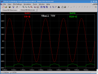
The attachment shows that T9-E (input to +Vrail output MOSFETs) seems to swing almost the full +Vrail to -Vrail (+75V to -75V) 68.1V to -61.9V, while T10-C (input to -Vrail MOSFETs) only swings a few volts -75V (-Vrail) to -68.3V. This despite a symetrical voltages +68.8V to -61.4V and +63.4V to -66.7V for T9-B and T10-B respectively.
Does this simulation concur with the actual module behaviour? If so, can anyone offer an explaination why there is such a big difference in the output of T9-E vs T10-C bevahiour?
Regards,
John L. Males
Willowdale, Ontario
Canada
15 October 2007 10:21
Official Quasi Thread Researcher
I have been snooping about with LTspice simulation until I have the time to make a special prototype board for the NMOS350. This will be the first of a few questions I like to ask the "experts" until I have a chance to confirm my simulation observations with a prototype board designed to allow me to "tinker".
The attachment shows that T9-E (input to +Vrail output MOSFETs) seems to swing almost the full +Vrail to -Vrail (+75V to -75V) 68.1V to -61.9V, while T10-C (input to -Vrail MOSFETs) only swings a few volts -75V (-Vrail) to -68.3V. This despite a symetrical voltages +68.8V to -61.4V and +63.4V to -66.7V for T9-B and T10-B respectively.
Does this simulation concur with the actual module behaviour? If so, can anyone offer an explaination why there is such a big difference in the output of T9-E vs T10-C bevahiour?
Regards,
John L. Males
Willowdale, Ontario
Canada
15 October 2007 10:21
Official Quasi Thread Researcher
Attachments
AndrewT said:Hi,
do you mean drain and source of the driver Fets?
Which schematic should we refer to?
Hi Andrew,
I am referencing the current NMOS350 schematic and T9-E to R20/R23/R24/R25 voltage (red trace) and T10-C to R22/R26/R27/R28 voltage (green trace).
Regards,
John L. Males
Willowdale, Ontario
Canada
15 October 2007 10:50
Official Quasi Thread Researcher
Hi Key,
you don't seem to understand quasi topology.
The Vgs of FETs behaves a bit like Vbe of BJTs.
The Vgs is nearly constant (around 4V instead of 600mV).
Now look at the gate voltages of T11 and T12.
Both are about 4V above their source voltages.
One is [-Vrail +4v] the other is [output voltage +4V].
As the -Vrail hardly moves you would expect that the FET source voltage to stay nearly constant and by topology, the gate voltage must also stay fairly constant. The variation on the gates is defined by the transconductance of the FETs. Look up the Id vs Vgs graph to see the voltage changes to turn the FET current up or down.
Now consider the upper FET bank.
The output rail moves with signal voltage. The FET source voltage must also move with the output voltage and this demands that the gate voltage must track the output voltage hence the swing from near rail to rail.
Does any of that make sense?
Look at it from another perspective:
the voltages across r20 and across r22 turn on the output FETs.If these two resistors pass the same current then the turn on voltage must be the same. If Vr20 = Vr22 then the voltage at the top of the respective resistors must track the rail they are attached to.
Hi Andrew,
One reason for my poking about with the simulation is for me to better understand the design.
The simulation does show a 5V difference between T11 and T12 Gate and Source is 5V. That is fine and that I understand.
The input signal is a 1KHz @ 1.9V P-P sine wave. Where I am not understanding is why there is such a difference in the gate voltages and lack of symmetry for the gate voltages with respect to the input signal? The simulation I posted is the drive gate voltage before the 27R0 gate resistors. This of course means the gates of the output MOSFETs are seeing a very different drive voltage that does not match the input signal symmerty.
Where my understanding seems to be lost is the lower MSOFET bank (-Vrail) voltage, does not swing in a symmetrical manner with respect to the upper MOSFET bank (+Vrail) voltage. All of the FETs have a 27R0 gate resistor. That said, I find the currents for R20 and R22 the same currents and symmetry, and alternating with each other. This makes sense as each alternates from 0ma to 30ma, where from 18ma to 30ma is the waveform and 0ma to 18ma appears to be the MOSFET threshold, but the voltages feeding the gates of the MOSFETs very different as I observed. So from a current perspective all looks fine for R20 and R22, but from a voltage perspective I am am not understanding.
Regards,
John L. Males
Willowdale, Ontario
Canada
15 October 2007 (11:17 -) 12:09
15 October 2007 12:22 Typoe correction. jlm
Official Quasi Thread Researcher
Re: Post #2429
Andrew,
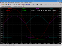
As a followup to Post #2429 I have attached the simulation output that shows the T9-E and T10-C voltages and the respective currents of R20 and R22. The simulation is with 75V rails and a 1.9 P-P sine wave input.
Regards,
John L. Males
Willowdale, Ontario
Canada
15 October 2007 12:40
Official Quasi Thread Researcher
Andrew,
As a followup to Post #2429 I have attached the simulation output that shows the T9-E and T10-C voltages and the respective currents of R20 and R22. The simulation is with 75V rails and a 1.9 P-P sine wave input.
Regards,
John L. Males
Willowdale, Ontario
Canada
15 October 2007 12:40
Official Quasi Thread Researcher
Attachments
Hi all,
what are the little currents in R20 before it switches fully off/on?
They seem to go from 2mA to zero hold at zero, then rise to 2mA again before turning fully on when the curent jumps to 18mA upto 30mA and this mimics the current in R22.
Are those little 2mA wings something to do with crossocer distortion and lack of output FET bias current?
Hi Key,
using a simulator to learn HOW a circuit works is going to be confusing.
Learn how it works by following a schematic and doing some calcualtions on what currents are flowing during different parts of the output waveform's cycle, or during quiescent when output current is zero.
I would suggest that sims are for fine tuning and investigating the details after you know what is happening.
If you don't know where to look or what to expect you're unlikely to stumble into the operation generalities.
this is absolutely crucial to the way Quasi complementary operates.As the -Vrail hardly moves you would expect that the FET source voltage to stay nearly constant and by topology, the gate voltage must also stay fairly constant.
Quasi,
Item 2 of Post #159 you explained the relationship of T2 and R6 (referenced as R7 in the posting).
Can you advise what will or will nor happen if R6 is set to 180K0 using 75V rails? I know an R6 value of 180K0 is not a practical value, but I am choosing an extreme value for R6 for this question on purpose. The motivation is to determine if LTspice or any other SPICE program and/or associated SPICE models can properly simulate your amplifier module.
Regards,
John L. Males
Willowdale, Ontario
Canada
16 October 2007 04:34
Official Quasi Thread Researcher
Hi Key,
is R6 the tail resistor on the input LTP?
2.7mA passing through the LTP to the CCS will try to generate 486V across 180k. No way.
A resistor that big virtually turns the LTP off.
Quasi said that you should aim to leave 12V across the CCS and never less than 5V. 75Vrail minus 486V dropped across 180k leaves -411V across the CCS, bordering on the impossible.
More likely, is that 180k will reduce theLTP current to 0.4mA and the mirror will try to equalise that current to 200uA per half.
I would try R6=15k for +-75Vrails
keypunch said:
[snip]
The motivation is to determine if LTspice or any other SPICE program and/or associated SPICE models can properly simulate your amplifier module.
AndrewT said:
A resistor that big virtually turns the LTP off.
75Vrail minus 486V dropped across 180k leaves -411V across the CCS, bordering on the impossible.
More likely, is that 180k will reduce theLTP current to 0.4mA and the mirror will try to equalise that current to 200uA per half.
Andrew,
Again the objective of R6 = 180K0 is not for real life module situation, but strickly for simulation purposes. The purpose of the R6 = 180K0 simulation is strickly to validate if LTspice, or any other SPICE program and/or the associated models are functioning correctly. No more.
That said, when I do set R6 = 180K0 in the LTspice simulation LTspice still shows a normal output waveform of about 62V with a 1.9V input signal. If the LTP is turned of should that not mean no output signal, much smaller output signal or a distorted waveform?
Regards,
John L. Males
Willowdale, Ontario
Canada
16 October 2007 13:28
Official Quasi Thread Researcher
Nmos200 can output 200W into 8 ohms with +/-67V rails, but can do this with 1 pair of IRFP460 ?
marus said:Nmos200 can output 200W into 8 ohms with +/-67V rails, but can do this with 1 pair of IRFP460 ?
The Nmos200 is designed to work with rails up to 50 volts. As well as other considerations this module uses a heatsink bracket instead of mounting output devices directly to the heatsink. This means the output devices may get too hot.
Cheers
Q
Temperature compensation for bias
Quasi, I finally matched the output MOSFETs for my NMOS200 (IRF840s) and got the bias current to even out amongst the 4 output devices. Matching was done to within +- 10mV of Gate to Source voltage. However, during the testing period, I noticed that the temperature compensation seems to over-compensate.
I set the bias at 60mA (30mV across the Source resistors) but when it warmed up, the reading dropped to 25mV. Is this normal? Output offset has been adjusted to around 1mV.
Re: Temperature compensation for bias
Your amp module seems to be working well, congratulations. I would not be concerned about the 5mV change. Most amplifiers need the output bias current set after the amp has had a chance to warm up so this change you are experiencing is quite normal. If you like adjust the initial (cold) bias current to 70mA and let it settle to around 62mA or wait until the amp has warmed (15 minutes) and then re-adjust to 60mA.
A 1mV output offset is perfect.
Cheers
Q
bawang said:Quasi, I finally matched the output MOSFETs for my NMOS200 (IRF840s) and got the bias current to even out amongst the 4 output devices. Matching was done to within +- 10mV of Gate to Source voltage. However, during the testing period, I noticed that the temperature compensation seems to over-compensate.
I set the bias at 60mA (30mV across the Source resistors) but when it warmed up, the reading dropped to 25mV. Is this normal? Output offset has been adjusted to around 1mV.
Your amp module seems to be working well, congratulations. I would not be concerned about the 5mV change. Most amplifiers need the output bias current set after the amp has had a chance to warm up so this change you are experiencing is quite normal. If you like adjust the initial (cold) bias current to 70mA and let it settle to around 62mA or wait until the amp has warmed (15 minutes) and then re-adjust to 60mA.
A 1mV output offset is perfect.
Cheers
Q
Thanks for the reply, Quasi. Further testing last nite revealed that once the bias has been set at 50mA (warm, after waiting for 30 mins w/out any signal), the cold bias current (immediately at startup) will be at around 90+mA, slowly decreasing to 50mA.
May be a good thing to prevent the output stage from self destruction in very hot conditions. However, this means that the bias has to be set higher initially....
May be a good thing to prevent the output stage from self destruction in very hot conditions. However, this means that the bias has to be set higher initially....
- Home
- Amplifiers
- Solid State
- Power amp under development