But I did state my requirements in a way I thought to be clear enough on my first post:
1) 12 single supply.
2) Must drive 50-75 ohm headphones to good levels, 600ohms if possible. So capable of large current.
3) Using output boost is an option.
4) It must use chips, not transistors or valves.
1) 12 single supply.
2) Must drive 50-75 ohm headphones to good levels, 600ohms if possible. So capable of large current.
3) Using output boost is an option.
4) It must use chips, not transistors or valves.
and why do you think the mini3 doesn't fit those requirements - which ones? - by how much margin? - which are more important?
the battery V can be 12 V if you like, if you looked at the schematic it does run on regulated 12 V when plugged in
the topology, chip choices, reasoning in the project description all seem relevant - but yes you may have to do some more engineering than just send the link to a Chinese manufacturing bidding site
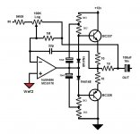
On ProAudioDesign people thought a simple circuit like that from mini3 wouldn't drive the pro caskets that will be used, from 25 to 75 ohms, up to good levels.
So I added an output boost, which ended up like this.
Maybe that answers your questions. Perhaps I was missing some option I didn't know, like a different chip or something, that would improve on this design.
I do not understand what China has to do with this.
So I added an output boost, which ended up like this.
Maybe that answers your questions. Perhaps I was missing some option I didn't know, like a different chip or something, that would improve on this design.
I do not understand what China has to do with this.
Attachments
running from 12 V single supply without bridging, DC-DC conversion is simply going to fail on Vswing for some headphones
some pro monitor headphones look like they really are expected to connect to a speaker power amp output by the V required
most headphones are being made with higher V sensitivity in the past few years - even the pro types
the AD8397 will drive 25 Ohms and up to as close to +/- 6 V peaks as possible
but you just won't get real world peak dynamic SPL out of a single 12 V supply amp with a number of respected headphones
So what do you think I should do? Use a chip with bridging? Which one?
It's interesting that (and this the second time I mention this today) the old-fashioned Nagra 4 and 4.2, which had a -10v regulated single supply, did move Beyer DT48 (25 ohm) and my AKG K-60 (50 ohms) to deafening levels in the headphone output. \
So why would a modern headphone not be moved to high levels using a 12v supply?
Another information which I think confirms what I said.
Have a look at the Rolls MX422:
http://www.rolls.com/pdf/M_MX422.pdf
Just single chips with no boost at all for the headphones.
Operates from what: 12-16v single supply.
Have a look at the Rolls MX422:
http://www.rolls.com/pdf/M_MX422.pdf
Just single chips with no boost at all for the headphones.
Operates from what: 12-16v single supply.
2 jcx
I've seen worse model than that. At the end it is not as important, as it does not model such effect as a gain drop in vicinity of zero output currents etc. A lot of job must be and was done on the real circuit to verify stability. I expected a phase lag fron the lmh part to be higher than modeled.
The question is different. Do you see now how R2 C3 modifies noise gain of the loop? Also, have you noticed feedforward chain whi allows partly compensate close pole of the lmh guy.
All you say is valid but does not take into account manipulations if the noise gain were made in the circuit.
Last edited:
So what do you think I should do? Use a chip with bridging? Which one?
Having differential output (if I understand you correctly), will make an amplifier incompatible with a lot of headphones, as three wire connection is very common.
yes bridged drive on the output requires 4 pins to the headphones - recabling to "balanced" connectors is popular among headphone audiophiles - but it isn't a generic solution
I did forget to mention output transformers - but quality audio output transformers with low distortion, low frequency extension may be a bit heavy for portable amps
I do have the complete circuit simmed in LTspice now - but the OPA1662 is apparently a Tina model - doesn't run in LTspice
I do see what the RC to gnd does - often called "noise gain compensation" - but you (unnecessarily) roll off you input with it too
and I still say you simply don't have safe margins with the datasheet numbers and graphs - the LMH spice model is too optimistic at high gain by factors of at least 2-3 , likely more for your local Av +11
you could look at my http://www.diyaudio.com/forums/soli...ain-composite-op-amp-circuits.html#post512806 thread or sample a few of the hundreds of posts I've made about spice, models, composite amplifiers, advanced compensation, loop stability... to get a better feel for my level of expertise on the subjects
and of course read the LMH6723 datasheet carefully for the multiple hints of how it falls short of the cfa ideal behavior, how corner frequency decreases with higher V gain
even the "bullet" specs
• 370 MHz Bandwidth (AV = 1, VOUT = 0.5 VPP) −3
dB BW
• 260 MHz (AV = +2 V/V, VOUT = 0.5 VPP) −3 dB
BW
Last edited:
2 jcx
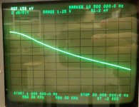
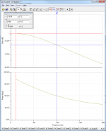
Here is a measured freq response with signal being injected into feedback midpoint (inverting input of the composite) via high-ish value resistor, to do not alternate noise gain of the circuit. Amplifier is loaded on a terminated 50Ohm line, so it sees 100Ohm load.
As you can see there is no peaking nowhere in vicinity of loop unity gain. The response changes somewhat with load impedance and a little bit more with output current, but stays reasonable. Sorry, have no time to do any more measurements.
There is also modeled response shown. It is somewhat different, but close enough to use it as a fist approximation. Nobody really expects that there 1-st level models can be used for the final stability evaluation.
Attachments
but you (unnecessarily) roll off you input with it too
It was an intention, to use this circuit as an input low pass filter at the same time. Don't see any problem with is, as a cut-off is rather high, around 400kHz. I would move it even lower, put large NP0 caps in 0603 are hard to get, and I was quire restricted it terms of area in the design.
and of course read the LMH6723 datasheet carefully for the multiple hints of how GBW decreases with higher V gain
even the "bullet" specs
jcx, the real world behavior or the opamp with given values was evaluated and taken into account. Circuit exhibits no sign of instability. What else are you looking for?
Last edited:
as I said - I don't consider the circuit, values shown to give a comfortable stability margin with my reading of the chip's datasheets
a single "working" example doesn't change that estimate - you may have board parasitics that help, may have gotten lucky in the typ vs min specs of your batch of chips...
I personally would not put that circuit into production with those values, can't recommend it to unsophisticated builders without specific high speed analog pro EE level experience and tools
the same or even more audio frequency loop gain could be had with alternative compensation and the same chips with much greater stability margins
Last edited:
jcx
Don't make a drama. First of all, nobody puts this design into a mass production. OP asked rather general question at the beginning, he got also rather generic answer from my side.
Yes, parasitic may help, as well as they can make situation worse. That is why a real world evaluation is required and important. If it would be a manufacturing project, the evaluation would be much more extensive. It would be made for several chips from different batches, over the temperate, over the supply voltage range ect. And yes, it would be made withing guarantied spec.
In this case I built only one sample of the circuit, pushed it a bit further than the spec quotes, proved that it is stable within the supply range I want and the load range I want. It shows desirable level of distortion. It is good enough for a such scale DIY project
Last edited:
Well, going back to my original and shown boosted output amp, what are the pro headphones I won't be able to drive with it, powered by 12-14.v8v?
Please specify brand and model.
Please specify brand and model.
Well, going back to my original and shown boosted output amp, what are the pro headphones I won't be able to drive with it, powered by 12-14.v8v?
Please specify brand and model.
All you need to do is look at manufacturer's specifications and you will have the answer to your questions.
you can search for "headphone sensitivity spreadsheet" - several have been made up, linked at Head-fi Head-Fi.org - Headphone forums and reviews for audiophiles , elsewhere
https://www.google.com/#q=headphone+sensitivity+spreadsheet
you have to define your amp's parameters
is it just do "as good as possible" with 12V single supply, simple circuits
or "I have to drive xxx and yyy headphones" and will use any circuit technique necessary
https://www.google.com/#q=headphone+sensitivity+spreadsheet
you have to define your amp's parameters
is it just do "as good as possible" with 12V single supply, simple circuits
or "I have to drive xxx and yyy headphones" and will use any circuit technique necessary
I would like to, but I know I won't be able to drive all headphones.
I will try several pro headphones and recommend those that work better with this supply. End of the story.
I will try several pro headphones and recommend those that work better with this supply. End of the story.
You know, for what you are asking for, a good LM386 circuit would do everything you want. It won't be as low noise as some of the exotic circuits you see around here, but it will drive just about any headphones you can think of. I made a headbanger variant as the first amp I ever made. I frequently load it up with some small PolkAudio satellite speakers of 8ohm impedance and it sounds great. Try that with a Cmoy.
It is not as clear as the amp that I use now, but in many respects, it drives my 32ohm Senns better. The only downside is the gain is too high for my tastes and it's clarity and dynamics go to the crapper unless you use a really nice pot or just do like I did and rig up a switch with some resistors instead of a volume pot.
It is a very simple single ended circuit. It runs fine on anything up to about 17v. It runs my little Polks from a 17v wallwart all day long.
LM386 - eek. I'd rather add an external feedback network to drop gain on a TDA2822M to 20 dB than use one of these crappy old things (which, btw, come in varying degrees of awfulness). And even that still is a non-ideal solution in term of noise, though it's a lot better already.
Re: the circuit in #23 - NJM4556A already delivers ~80 mA (rms) max. Is 2 Vrms into 25 ohms enough? Also, the midpoint of the 10µ caps must go to boosted output for bootstrapping to work. Make sure booster transistors run a decent amount of Iq (like 2-3 mA min, the more the merrier), otherwise performance may easily be worse than unboosted.
Re: the circuit in #23 - NJM4556A already delivers ~80 mA (rms) max. Is 2 Vrms into 25 ohms enough? Also, the midpoint of the 10µ caps must go to boosted output for bootstrapping to work. Make sure booster transistors run a decent amount of Iq (like 2-3 mA min, the more the merrier), otherwise performance may easily be worse than unboosted.
Last edited:
That IC looks interesting, but I can't use with a pot before it, because I would be taking the input from the main output chip.
For not I will try it a simple 4556 and see how it does.
For not I will try it a simple 4556 and see how it does.
- Status
- Not open for further replies.
- Home
- Amplifiers
- Headphone Systems
- Portable headphone amp