Member
Joined 2002
Bas Horneman said:
Nope...we need a little more feedback from others to try and make it better.
What software are you using to creat this schematic ? I use eagle.
Is there a such program that simulatescircuit'swith Tube's and fet's...?
Hey Guys,
Great thread! I've done a PCB layout of the Aikido, also ... I haven't actually had the boards cut, though.
I was going to wire-twist the the heater leads, and solder them to the bottom of the PCB at the tube socket. This keeps the leads away from the PCB traces, and also gives room to put a ferrite bead.
I thought about using DC heaters, but it uses so much power - the CCS for the heaters need to drop a couple volts (4-5V), which dumps more heat on my heatsinks, which are already hot enough! DC heaters also require a sepeate transformer just for the heaters, which complicates chassis layout for an already difficult system.
This is a great thread. I love my hardwire Aikido (6Dj8).
K.
Member
Joined 2002
Kashmire said:Hey Guys,
Great thread! I've done a PCB layout of the Aikido, also ... I haven't actually had the boards cut, though.
I was going to wire-twist the the heater leads, and solder them to the bottom of the PCB at the tube socket. This keeps the leads away from the PCB traces, and also gives room to put a ferrite bead.
I thought about using DC heaters, but it uses so much power - the CCS for the heaters need to drop a couple volts (4-5V), which dumps more heat on my heatsinks, which are already hot enough! DC heaters also require a sepeate transformer just for the heaters, which complicates chassis layout for an already difficult system.
This is a great thread. I love my hardwire Aikido (6Dj8).
K.
Pictures of your done board ?
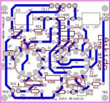
Latest version
Latest version...
 Compromised URL removed by Moderation
Latest version...
Compromised URL removed by Moderation
Last edited by a moderator:
Member
Joined 2002
Re: Latest version
Id like to download the software you are using for this board layout and show you some changes. .. what is the software.. OR if you could email me and ill show you where you could change some stuff. 😀
J'
Bas Horneman said:Latest version...
Id like to download the software you are using for this board layout and show you some changes. .. what is the software.. OR if you could email me and ill show you where you could change some stuff. 😀
J'
Last edited by a moderator:
Jason,
Why not discuss the changes here? I'm suprised how little feedback and suggestions were getting on this board!
Cheers,
Bas
Why not discuss the changes here? I'm suprised how little feedback and suggestions were getting on this board!
Cheers,
Bas
Member
Joined 2002
Hi Jason,
Well like I've said in previous posts. The resistors are slanted for a purpose. R2/R7 are grid stoppers and should be as close to the pin as possible. The others can be straight. But why would you want to make signal paths longer just so the pcb looks nicer?
R2 actually needs to go more to the right so that the path to pin 2 is shorter...like R7 is to pin7.
I don't have the software....bonny_kjs has.
Cheers,
Bas
Bas Horneman said:Jason,
Why not discuss the changes here? I'm suprised how little feedback and suggestions were getting on this board!
Cheers,
Bas
Some of us ain't qualified.
sheldon
Just some thoughts. These may neither be good nor practical.
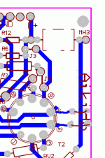
[1] 6.3V filament power. Can the power input pads be placed between the two tubes? Put the pads where J2 and J3 are and eliminate J2 and J3.
[2] If we do [1] above, we have to move R12 and C1 south of the tubes. This will eliminate the long trace underneath J2 and J3 and also the long trace on the right side of the board, connecting R10 and C1.
[3] If we do [1] above, we can also eliminate J1 and J6 and relocate the power input pads to where J1 is currently.
[4] Question: what kind of cost are we looking at here? How much more for a 2-sided board? I can't really tell, but there is something about how the GND is layed that bugs me.
[5] Another trick to shorten signal path is to locate and subsequently solder components on both sides. Just something to consider. The downside is that you need to be much more careful when soldering.
Excellent suggestion.[1] 6.3V filament power. Can the power input pads be placed between the two tubes? Put the pads where J2 and J3 are and eliminate J2 and J3.
Bingo again.2] If we do [1] above, we have to move R12 and C1 south of the tubes. This will eliminate the long trace underneath J2 and J3 and also the long trace on the right side of the board, connecting R10 and C1.
Si ...[3] If we do [1] above, we can also eliminate J1 and J6 and relocate the power input pads to where J1 is currently.
Don't know. I believe making 2 sided board is not an option for bonny_kjs.[4] Question: what kind of cost are we looking at here? How much more for a 2-sided board? I can't really tell, but there is something about how the GND is layed that bugs me.
The gnd bugs me as well...but I thought it's enough of a bus so that it might just work..but when thinking ground...apparently one has to think current...and both cathode resistors dump the current through the bottom part and has to go all the way past the input "all the way" too the gnd part up north. (Excuse my pseudo tech babble) Some kind of star earth would be nice.
Then you might as well go point to point...😀[5] Another trick to shorten signal path is to locate and subsequently solder components on both sides. Just something to consider. The downside is that you need to be much more careful when soldering.
Agent.5 AFAIC you get promoted to the yellow belt in Aikido. That means you are the Doyen now.
Then you might as well go point to point...😀
Agent.5 AFAIC you get promoted to the yellow belt in Aikido. That means you are the Doyen now.
How about a layout that have some components connected to the tube sockets and the rest on a PCB?
quote:
[3] If we do [1] above, we can also eliminate J1 and J6 and relocate the power input pads to where J1 is currently.
Si ...
Please reconsider.
I need J1, J6 to allow the use of an ECC99 or 12BH7 for my application as an output tube driver. More swing available than a 5687 for driving a 300b or 845. Also for an electrostatic headphone driver.
dshortt9 said:quote:
[3] If we do [1] above, we can also eliminate J1 and J6 and relocate the power input pads to where J1 is currently.
Si ...
Please reconsider.
I need J1, J6 to allow the use of an ECC99 or 12BH7 for my application as an output tube driver. More swing available than a 5687 for driving a 300b or 845. Also for an electrostatic headphone driver.
Thanks for the insight. I have said this in a prior post and I like to re-emphasize it again. In order to accommodate all the different tubes that people will be using:
i think this circuit really needs two separate boards. Either both are PCBs, or one PCB and one p2p. Locate the tube sockets on one board and the rest of the components on the other and joint both boards in a L shape, using an edge connector.
Could you be more specific?How about a layout that have some components connected to the tube sockets and the rest on a PCB?
Yes, there are people that prefer octal over anything else as well as your 7N7,7AF7.
It seems as if tube sockets and filament connections should be on one board and the rest of the circuitry on the mother board.
This will, however increase the cost significantly.
It seems as if tube sockets and filament connections should be on one board and the rest of the circuitry on the mother board.
This will, however increase the cost significantly.
- Home
- Amplifiers
- Tubes / Valves
- Poll..anyone interested in an Aikido linestage PCB group buy?