PMA CFA - current feedback power amplifier with +/-25V to +/-55V dc supply range
Intro
This project has started in the beginning of 2016 for the reason that I was interested in a current feedback topology (CFA) behaviour. The current feedback concept is well described in Renesas company application notes. For those who are interested, I recommend to download the application notes that I have linked below. I could hardly say anything more.
https://www.renesas.cn/cn/zh/document/apn/an9420-current-feedback-amplifier-theory-and-applications
https://www.renesas.cn/cn/zh/docume...ersus-current-feedback-operational-amplifiers
The goal was to design a simple and robust amplifier that would be able to drive difficult loads, would be stable and would have balanced time and frequency domain characteristics. The lowest nonlinear distortion was not the design goal, just to keep it inaudible.
Another goal was to make it working with a wide range of power supply voltages, here namely from 2 x 25V to 2 x 55 V.
The amplifier, with working title ACCE3, has been reliably operated for years, without a single problem.
Circuit design
Amplifier schematics is as follows. The circuit is complete, with part numbers and values.

Q1-Q4 make a CFA input stage, with low impedance inverting input into R14/R15 common junction. Q5-Q8 make a VAS stage, with quite high current through Q5/Q6.
Output devices are 3 pairs of robust OnSemi MJL21194/93. Drivers are MJE15030/03. Similarly as in case of my PA4 amplifier, the rugged and reliable amplifier was my goal.
Supply voltage was tested at 2 x 25V and 2 x 55V, with no change in the circuit. The amplifier can easily drive 2 ohm load with 2 x 25V, staying completely safe. With 2 x 55V, I would recommend for the load impedance not to be lower than 3 ohm.
IC1, DC servo, is to be OPA177 opamp, for the reason of excellent DC parameters and for the reason of low idle current of 1.3 mA. This is necessary to cover wide supply range of 2 x 25V to 2 x 55V without unwanted high voltage drop across R32 and R33.
The amplifier is stable without an output coil, however, for safety reason I would recommend to add a parallel R//L combination 1uH//6R8 behind the X2-1 (X2-2) output terminal.
Construction notes
The amplifier is strictly dual-mono, channels do not share any common ground point, so no ground loops are created. The power supply has one transformer with separated secondary winding for left and right channel. It has separate center-tapped bridge rectifiers with capacitor banks of 2 x 14100 uF for each channel, as can be seen from the photos.
Voltage drop across 0R22 emitter resistors (R25 etc.) is set between 15mV - 22mV, which makes idle current per transistor equal to 68mA - 100mA.
Photos of the amplifier
The amplifier with 2 x 25V dc supply built in my old Fischerelektronik 19” 3U 20+ years old prototype case can be seen below:

And this is the more detailed photo of one module built in another amplifier with 2 x 55V PSU.

Basic specifications
•Output power 2 x 200W/4ohm with 2 x 55V supply, 2 x 40W/4ohm with 2 x 25V supply, THD 1%
•Frequency roll off (-3dB) 225kHz
•Harmonic distortion <0,02%/1kHz/100W/4ohm (2 x 55V PSU)
•CCIF 19kHz+20kHz 0,01%/30W/4ohm (2 x 55V PSU)
•Rise time of step response 1.4us
•Gain 27dB
•S/N ratio 94dB/2,83V/BW20kHz/linear, 114dB at full swing (2 x 55V PSU)
•minimum load impedance 2 ohm resistive/complex with 2 x 25V supply, 2 ohm resistive or 3 ohm complex with 2 x 55V supply
Measurements
Amplitude and phase response within 20Hz – 40kHz range

We can see gain of 27.1dB and amplitude and phase response flat in the audio band.
Step response

Rise time (10% - 90%) of the step response is 1.28us when measured with the fast function generator with 10ns rise time. This indicates to 273kHz/-3dB amplifier bandwith.
Response to 10kHz square

Response to square wave does not depend on signal amplitude, it is level invariant, thanks to CFA topology. This was measured with a generator with about 2 us rise and fall time.
Distortion measurements with 2 x 25V supply
THD+N vs. power at 1kHz into 4ohm load

I do not have an autoranger, so this was measured with 2 settings of ADC input range, 10V and 60V. This is for the reason that at 60V range the system noise is higher than amplifier noise and thus we get too high THD+N numbers at low power, due to measuring system intrinsic noise.
We can see that THD = 1% is at 40W and that the distortion knee is about 27W.
Comparison of THD+N vs. power at 1kHz into 2.2 ohm and 4 ohm load (and comparison of measurement vs. simulation)
measurement simulation
THD+N = 1% is at 40W/4ohm and 60W/2.2ohm. There is no extreme rise of distortion into 2.2ohm load, the amplifier has no problem with it. And as always, simulated result is more optimistic than the real life result.
THD vs. frequency at 30W into 2.2ohm load

Distortion stays below 0.1% up to 22kHz. Below 100Hz we can see effect of heavy power supply load (ripple) due to high load current.
19+20kHz CCIF IMD

Overload recovery according to IEC60286-3 (overload recovery time)
First. the definition. I find this test extremely important!

and, the measurements with 20Hz and 1kHz signals


Distortion measurements with 2 x 55V supply

Measurements with 2 x 55V supply were done 4 and more years ago, with another measuring system, that was unable to make stepped THD and THD+N vs. power measurements properly. Please let me show only 100W/4ohm/1kHz spectrum.
Conclusion
The amplifier has proven to be reliable in operation since 2016. It is robust and able to drive difficult loads, while tested into complex load and R//C load.
https://pmacura.cz/pmacfa.htm
_____________________________________________________________________________________________________________________________________________________
Edit: Gerber files and BOM
I am attaching Gerber files and BOM which applies to the amplifier shown in the photos above and which were used for PCB production. Please note there is one wire jumper on the PCB shown in the pdf brd file. Gerber files updated with vertical power transistor packages!
Intro
This project has started in the beginning of 2016 for the reason that I was interested in a current feedback topology (CFA) behaviour. The current feedback concept is well described in Renesas company application notes. For those who are interested, I recommend to download the application notes that I have linked below. I could hardly say anything more.
https://www.renesas.cn/cn/zh/document/apn/an9420-current-feedback-amplifier-theory-and-applications
https://www.renesas.cn/cn/zh/docume...ersus-current-feedback-operational-amplifiers
The goal was to design a simple and robust amplifier that would be able to drive difficult loads, would be stable and would have balanced time and frequency domain characteristics. The lowest nonlinear distortion was not the design goal, just to keep it inaudible.
Another goal was to make it working with a wide range of power supply voltages, here namely from 2 x 25V to 2 x 55 V.
The amplifier, with working title ACCE3, has been reliably operated for years, without a single problem.
Circuit design
Amplifier schematics is as follows. The circuit is complete, with part numbers and values.
Q1-Q4 make a CFA input stage, with low impedance inverting input into R14/R15 common junction. Q5-Q8 make a VAS stage, with quite high current through Q5/Q6.
Output devices are 3 pairs of robust OnSemi MJL21194/93. Drivers are MJE15030/03. Similarly as in case of my PA4 amplifier, the rugged and reliable amplifier was my goal.
Supply voltage was tested at 2 x 25V and 2 x 55V, with no change in the circuit. The amplifier can easily drive 2 ohm load with 2 x 25V, staying completely safe. With 2 x 55V, I would recommend for the load impedance not to be lower than 3 ohm.
IC1, DC servo, is to be OPA177 opamp, for the reason of excellent DC parameters and for the reason of low idle current of 1.3 mA. This is necessary to cover wide supply range of 2 x 25V to 2 x 55V without unwanted high voltage drop across R32 and R33.
The amplifier is stable without an output coil, however, for safety reason I would recommend to add a parallel R//L combination 1uH//6R8 behind the X2-1 (X2-2) output terminal.
Construction notes
The amplifier is strictly dual-mono, channels do not share any common ground point, so no ground loops are created. The power supply has one transformer with separated secondary winding for left and right channel. It has separate center-tapped bridge rectifiers with capacitor banks of 2 x 14100 uF for each channel, as can be seen from the photos.
Voltage drop across 0R22 emitter resistors (R25 etc.) is set between 15mV - 22mV, which makes idle current per transistor equal to 68mA - 100mA.
Photos of the amplifier
The amplifier with 2 x 25V dc supply built in my old Fischerelektronik 19” 3U 20+ years old prototype case can be seen below:
And this is the more detailed photo of one module built in another amplifier with 2 x 55V PSU.
Basic specifications
•Output power 2 x 200W/4ohm with 2 x 55V supply, 2 x 40W/4ohm with 2 x 25V supply, THD 1%
•Frequency roll off (-3dB) 225kHz
•Harmonic distortion <0,02%/1kHz/100W/4ohm (2 x 55V PSU)
•CCIF 19kHz+20kHz 0,01%/30W/4ohm (2 x 55V PSU)
•Rise time of step response 1.4us
•Gain 27dB
•S/N ratio 94dB/2,83V/BW20kHz/linear, 114dB at full swing (2 x 55V PSU)
•minimum load impedance 2 ohm resistive/complex with 2 x 25V supply, 2 ohm resistive or 3 ohm complex with 2 x 55V supply
Measurements
Amplitude and phase response within 20Hz – 40kHz range
We can see gain of 27.1dB and amplitude and phase response flat in the audio band.
Step response
Rise time (10% - 90%) of the step response is 1.28us when measured with the fast function generator with 10ns rise time. This indicates to 273kHz/-3dB amplifier bandwith.
Response to 10kHz square
Response to square wave does not depend on signal amplitude, it is level invariant, thanks to CFA topology. This was measured with a generator with about 2 us rise and fall time.
Distortion measurements with 2 x 25V supply
THD+N vs. power at 1kHz into 4ohm load
I do not have an autoranger, so this was measured with 2 settings of ADC input range, 10V and 60V. This is for the reason that at 60V range the system noise is higher than amplifier noise and thus we get too high THD+N numbers at low power, due to measuring system intrinsic noise.
We can see that THD = 1% is at 40W and that the distortion knee is about 27W.
Comparison of THD+N vs. power at 1kHz into 2.2 ohm and 4 ohm load (and comparison of measurement vs. simulation)
measurement
simulation THD+N = 1% is at 40W/4ohm and 60W/2.2ohm. There is no extreme rise of distortion into 2.2ohm load, the amplifier has no problem with it. And as always, simulated result is more optimistic than the real life result.
THD vs. frequency at 30W into 2.2ohm load
Distortion stays below 0.1% up to 22kHz. Below 100Hz we can see effect of heavy power supply load (ripple) due to high load current.
19+20kHz CCIF IMD
Overload recovery according to IEC60286-3 (overload recovery time)
First. the definition. I find this test extremely important!
and, the measurements with 20Hz and 1kHz signals
Distortion measurements with 2 x 55V supply
Measurements with 2 x 55V supply were done 4 and more years ago, with another measuring system, that was unable to make stepped THD and THD+N vs. power measurements properly. Please let me show only 100W/4ohm/1kHz spectrum.
Conclusion
The amplifier has proven to be reliable in operation since 2016. It is robust and able to drive difficult loads, while tested into complex load and R//C load.
https://pmacura.cz/pmacfa.htm
_____________________________________________________________________________________________________________________________________________________
Edit: Gerber files and BOM
I am attaching Gerber files and BOM which applies to the amplifier shown in the photos above and which were used for PCB production. Please note there is one wire jumper on the PCB shown in the pdf brd file. Gerber files updated with vertical power transistor packages!
Attachments
Last edited:

I had a go at simulating this - I found changing to a CFP output would increase distortion a bit and the phase margin might be marginal... Its not clear from the photos whether the feedback pick-off point is from the actual output node (if not you might be adding distortion from non-linear IR trace voltages).
I had a go at simulating this - I found changing to a CFP output would increase distortion a bit and the phase margin might be marginal... Its not clear from the photos whether the feedback pick-off point is from the actual output node (if not you might be adding distortion from non-linear IR trace voltages).
Simulation shows lower phase margin (below), however the real world amplifier is pretty stable. I am not sure how well a common loopgain stability method works with CFA amplifiers. I tend to believe the simulators in a limited degree, especially in case of stability and HF non-linearity.

BTW Are you planning to share gerber files for PCB?
Possibly yes. I need to go through my archive, because the files I have on my new PC (installed after the amp was designed) do differ a bit, as I was thinking about some modifications, but I will not post the files that are not verified in a real world application. So, I have to review the files in my old PC, if there is a real interest for Gerbers and BOM.
Regarding the minimum load, I was quite conservative in my post #1. In fact, with 2 x 25V, complex load of 2ohm with dips below 2ohm is no issue. With 2 x 55V supply, 2 ohm resistive load is a non-issue. 2 ohm complex load is just at the limit, so I would say 3 ohm complex load would be a minimum. Some simulated plots below.
2 ohm complex load circuit

SOA with 2 ohm complex load, 2 x 55V PSU

SOA with 2 ohm resistor, 2 x 55V PSU

Please note how complex load is much more demanding (and dangerous) re transistor stress and please take into account that testing amplifiers with resistors only is completely inadequate.
2 ohm complex load circuit
SOA with 2 ohm complex load, 2 x 55V PSU
SOA with 2 ohm resistor, 2 x 55V PSU
Please note how complex load is much more demanding (and dangerous) re transistor stress and please take into account that testing amplifiers with resistors only is completely inadequate.
Thanks for sharing, note that there is discrepancy between the discussed CFA in the papers and your implementation. Your implementation is in line with later accuphase and NAD et al. In terms of feedback math the discussed CFA is in line with some Jeff Rowland implementations. More gain in the input stage or more gain in the VAS is the game played. Your running your input stage quite hot for those cute THD numbers but your VAS seems upto the task, thanks again. Amp stability is also a very interesting arena, take the discussed stability criterion and math as first principles. Some CFA amps resemble early non symmetrical amplifiers before the advent of LTPs
Last edited:
At this point I don't see any reason to build this amplifier.. We have better amplifiers that are worth building. (SA2014, Wolverine, FukAmp)
For those who might be interested I have added Gerber files and BOM to the post #1.

Last edited:
PMA
Thank you very much for adding gerber files
Perhaps I will use it in the near future.
Once again - great respect for sharing the complete project - with simulation and measurement results
A very professional approach to the DIY community
Thank you
Thank you very much for adding gerber files
Perhaps I will use it in the near future.
Once again - great respect for sharing the complete project - with simulation and measurement results
A very professional approach to the DIY community
Thank you

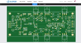
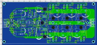
Normally it was cropped in production to board dimensions 200 x 75 mm and the board was produced exactly to 200 x 75, without the area below the power transistors and without their package outline. These are exactly the files as used in 01/2017 to produce the boards. I can change transistor packages to vertical, that will not overlap the free space.
Your image was produced by yourself or by the PCB manufacturer? If it is your, it might be a product of Gerber view only.
Your image was produced by yourself or by the PCB manufacturer? If it is your, it might be a product of Gerber view only.
I quickly checked your PCB in Gerber Viewer ( JLC PCB )
Something is wrong ....I mean the material outside the outline of the PCB itself - under the power transistors...
Ok thanx fou your reply
This image is produced by myself .
Please check again post #1 and let me know, I have updated the Gerber plots with vertical power transistor packages (file ACCE3-1.zip). It should be OK now. My apologies for possible inconvenience.
BTW, the photo below shows that with original (old) files the board was really produced to correct 200 x 75, see the package outline cut at the board edge. OK, new corrected files available in post #1.

Last edited:

Kindly share the real numbers behind Harmonic distortion <0,02%/1kHz/100W/4ohm (2 x 55V PSU)
What's the difference between the THD numbers on both Channels at start up and after warm up, did you match the transistors and are they from similar batch numbers? How much is the THD drift between different measurements
What's the difference between the THD numbers on both Channels at start up and after warm up, did you match the transistors and are they from similar batch numbers? How much is the THD drift between different measurements
The input stage isn't usually run very hot maybe 20db at most, your THD measurements for both channels wont be the same (Which BC546 are you using). Dartzeel in their non switching amplifier for midrange and highs does 20db for input stage. The amplifier output is self protecting from overcurrent and is biased around 100mA
Last edited:
- Home
- Amplifiers
- Solid State
- PMA CFA - current feedback power amplifier with +/-25V to +/-55V dc supply range