Are you serious??? Smaller distance results in lower inductance of parallel wires! Back to school, Sir 🙂You did implement 5mm distance between the two conductors, in your pic the cables are stuck together at one mm distance, that s typically setting the wrong parameters to be on point.
And, spacing cannot be smaller than wire diameter.
Guys, I am leaving the thread and give a space for your DIY improvements.
better calculator
https://www.eeweb.com/tools/parallel-wire-inductance/
0.1uH is enough if the amp is stable to 10nF in the simulator -> square wave test near full power
https://www.eeweb.com/tools/parallel-wire-inductance/
0.1uH is enough if the amp is stable to 10nF in the simulator -> square wave test near full power
Actually i didnt even use a square wave to simulate this amp, it oscillate even with a regular sine signal, this with Pavel s own dummy load, at 0.5uH parasistic inductance in serial it s "stable".
Also the inductance calculator is for perfectly straight cables, in the amp pics the conductors are not straight at all, there s a U shape
to get to the rear panel, so computations in the calculator are forcibly not accurate in respect of the real implementation.
Edit : If a regular miller compensation is implemented instead of the shunt compensations then 150-200pF are necessary
to render the amp stable in the test dummy load, that s quite high values, 100pF were enough for a single differential LIN
of the so called blameless topology and using this same load.
Last edited:
Are you serious??? Smaller distance results in lower inductance of parallel wires! Back to school, Sir 🙂
Guys, I am leaving the thread and give a space for your DIY improvements.
Well, dunno if i have to get back to school, guess that if i do so i will be remembered that 46dB GNFB at 20kHz is a recipe
for a stability disaster, that s exactly what render this amp instable, seems that there s a misconception that CFAs can have
higher GNFB ratio at high frequencies, hence this unrealistic value.
To get the amp stable in your dummy load the two 220pF shunt capacitors have to be increased to 2.2nF, the step response is not even worse with such high values and this change nothing to the THD at 1kHz.
Hello PMA,
Please, don't leave yet, I have a little question:
Is there any particular reason for such high VAS current (roughly calculated 33mA)?
And if You'll find some more time, another one, about post #38 (#38).
I cant figure out, how C1 and C2 can decrease phase shift around 1MHz.
Maybe there is some interaction between EF2 negative input resistance... ... and there are no usual base stoppers ..
I'll probably figure this out later, but any explanation from You would be helpful.
Please, don't leave yet, I have a little question:
Is there any particular reason for such high VAS current (roughly calculated 33mA)?
And if You'll find some more time, another one, about post #38 (#38).
I cant figure out, how C1 and C2 can decrease phase shift around 1MHz.
Maybe there is some interaction between EF2 negative input resistance...
... and there are no usual base stoppers ..I'll probably figure this out later, but any explanation from You would be helpful.
Is there any particular reason for such high VAS current (roughly calculated 33mA)?
And if You'll find some more time, another one, about post #38 (#38).
I cant figure out, how C1 and C2 can decrease phase shift around 1MHz.
High VAS current is chosen for the reason of both stability and ability to feed drivers with high impulse current when input has high dv/dt.
Regarding C1 and C2, as already explained by @EdGr , they shift OLG pole and modify slope of OLG response. It is a shunt compensation to VAS.
OLG with C1, C2 = 0pF

OLG with C1, C2 = 220pF

I am sorry I am not able to give any better or more clear explanation. The loopgain in post #38 covered it.
BTW, I measured Rout, at rear panel binding posts it makes 0.025 ohm.
Comparison of FR into 4R7 resistor and my dummy load (please note the Y-axis range is +0.21dB, -0.32dB full scale)


Last edited:
Measurements of output impedance
Most of all I use current injection method

Driving amp (or channel) injects sine current through the 10 ohm resistor to the measured channel. I use 10Vpeak driving voltage which makes 1Apeak current. Voltage is measured at the measured channel terminal and Zout calculated according to Ohm law.
Zout at 1kHz

We get 20mVp approx. from 1Ap current, so Zout = 0.02 ohm at 1kHz.
Zout at 21.5kHz

We get 34mVp from 1Ap current, so Zout is 0.034 ohm at 21.5kHz. Please note the inductive phase shift, Zout = Rout + jwL
Most of all I use current injection method
Driving amp (or channel) injects sine current through the 10 ohm resistor to the measured channel. I use 10Vpeak driving voltage which makes 1Apeak current. Voltage is measured at the measured channel terminal and Zout calculated according to Ohm law.
Zout at 1kHz
We get 20mVp approx. from 1Ap current, so Zout = 0.02 ohm at 1kHz.
Zout at 21.5kHz
We get 34mVp from 1Ap current, so Zout is 0.034 ohm at 21.5kHz. Please note the inductive phase shift, Zout = Rout + jwL

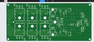
@Astaro thank you for the gerbers, great layout, however see the screen shot of render (underside), it looks like the mask is covering the solder pads. It does not look like the first image you posted?
Also R16 & R17 appear to be in the way of the driver transistors to lie flat if you get me...
Also R16 & R17 appear to be in the way of the driver transistors to lie flat if you get me...
Attachments
It's in the archive not in gerber format, but *.Laythank you for the gerbers
Either this viewer misunderstood the format so badly, or you forgot about the layer with the solder pad when making gerberit looks like the mask is covering the solder pads
so the resistors are soldered on the board, and the board is connected through 6-8 mm brass posts to the radiator. That is, there is still a couple of mm distance between the transistor and the resistor.Also R16 & R17 appear to be in the way of the driver transistors to lie flat if you get me...
The transistors on this side should be on the radiator. The board is also parallel to the radiator on brass pillars
Astro, in post #53 you published your 'Gerbers' for us to use. So the board cannot be used as is?
Forgive my ignorance but which software do I ned to fix the connection issue? I just want a working PCB Gerber for JLPCB. Their gerber viewer works just fine.
Got it regarding component spacing and pillars 😉
Forgive my ignorance but which software do I ned to fix the connection issue? I just want a working PCB Gerber for JLPCB. Their gerber viewer works just fine.
Got it regarding component spacing and pillars 😉
Really? How do they compare in the overload recovery test? How about the difficult load tests? Just because an amplifier measures well in certain "figure of merit" tests into a resistive or other easy load is not necessarily the final arbiter of amplifier quality. There is much more that can be and should probably be measured, such as Bob Cordell points out in chapter 16 of the 2nd edition of his book on amplifier design.At this point I don't see any reason to build this amplifier.. We have better amplifiers that are worth building. (SA2014, Wolverine, FukAmp)
- Home
- Amplifiers
- Solid State
- PMA CFA - current feedback power amplifier with +/-25V to +/-55V dc supply range