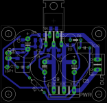
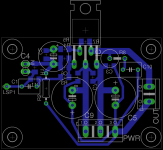
thanks for the help guys, new design is attached, i changed quite a lot of stuff, removed the psu for the time being, cleaned the input stage, used 1206 smd for some resistors and caps, changed the grounding. the board is 2.1x1.5 inch. Please let me know if there are any issues with it.
Attachments
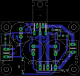
thanks for the help guys, new design is attached, i changed quite a lot of stuff, removed the psu for the time being, cleaned the input stage, used 1206 smd for some resistors and caps, changed the grounding. the board is 2.1x1.5 inch. Please let me know if there are any issues with it.
Already much better!
You should have some PCB area available under the LM1875 chip so that you can have R7 between chip pins 2 and 4.
No need to jump input pin1 track with cap4. Turn the input connector 180deg to have the input gnd on the top pin of it. This way you can get a minimalistic input ground and micro size input/feedback circuit with most of those parts under the cap4. Cant get much smaller than that. Then jump tracks with the R2 if needed...
Others may have even better ideas...
I couldn't fit in r7 between the chip pins even with an 0805 resistor, didn't want to go smaller than that. moved the dimension a bit to accommodate r7, hopefully it doesn't cause issues with mounting the heat sink. the gap between the chip and the border is about 0.1".
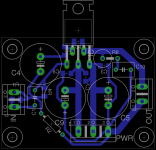
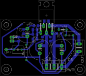
I also rotated the input socket by 180, input ground has become smaller. also moved C1 closer. image is attached.
I also rotated the input socket by 180, input ground has become smaller. also moved C1 closer. image is attached.
Attachments
R7, that is exactly what i meant.
I would still:
- Turn R5 horizontaly to get shorter leads to it.
- Make the input star point around C4 bottom pin.
- Make it look sexy and move R4 up below R5, connect to the star point in C4.
- Add the R2 and C2 from the circuit in post #4, place them all under Cap C4, use MLCC for C2.
- For audiophile sex appeal i would put a parallel MLCC to the C4.
- C1 needs more space around it. Some like to use a bigger size capacitor there, for example 10uF (50V) size 11x7.2mm. Also for audiophiles, put a parallel MLCC under it.
Good work so far.
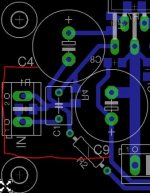
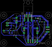
did most of the changes. created more space around c1, added a pad for larger caps, now it supports 5mm and 10mm grid caps. can handle width of 7.5mm
added input filter r3 and c6
couldnt add a ceramic bypass smd cap to the input cap c1, 1206 doesnt have enough space to allow a track below it. I guess i can add a small leaded one to the bottom of the board later.
added the guard track.
added input filter r3 and c6
couldnt add a ceramic bypass smd cap to the input cap c1, 1206 doesnt have enough space to allow a track below it. I guess i can add a small leaded one to the bottom of the board later.
added the guard track.
Attachments

Slowly but surely...
Some sexyness is still neened, IMO.
Turn Cap6 parallel to R4 (and R5).
Also turn R3 parallel to them and put them all in a nice even row one abowe the other. Sexy huh?
You can jump the tracks later with the R2. You dont need to run its lead between C1 pins. You will see ones we get there...
I would also turn C1 horizontally, and then add the audiophile MLCC parallel under it.
The audio input star point can be physically located directly ATT the C4 bottom pin. Move it there.
If too tight, make the PCB a bit wider, or actually you should, because I will next totally rearange your Power input circuit and Speaker output circuit... 😉
I might want to use a 2.54mm pin terminal as the input connector for the audio. No need for a heavy duty screw terminal there... Advantages, you will save PCB area for the bigger C1, leads are closer (better noise performance) and so on...
Last edited:
Nice!
R3 can be connected to C6 the same way you as have connected R4 to it.
R1 can be a terminator to the input connector so no need to separately trace it to your star.
Take C1 input from the R1, not from the input connector.
Increase PCB width so that you can have R2 vertically between C1 and C8.
Move R5 just a little bit to the left so that, you know what...
Thats it. Input circuitry should now be as sexual as it can get.
If fellow colleagues have an opinion about this, now is the time to react!
...Before I move to the Power park...
Yes!
Put the R5 really in line with the rest R3,4, C6... You have the same inductance in the wires so the position is not critical any longer. Sexyness is important.
You see, if it looks good, it sounds good...
And now put the parallel MLCC to the C1.
Also,
see how the input ground now forms a nice tight area?
You can further lower the wire impedance and make it a close to zero impedance reference point for the input circuitry by improving the former "star point". Make the ground wires as wide as possible, or even a copper pour.
That should complete the input side.
Last edited:
C3 and C8 can't work as HF decoupling capacitors with those very long traces.
The Signal Input trace does not follow the Signal Return trace. You have a large loop area in there.
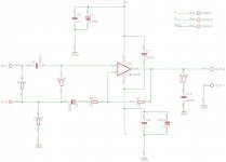
I can't find R22, I have found C2 & C6, but they are not on the sch.
The Signal Input trace does not follow the Signal Return trace. You have a large loop area in there.
I can't find R22, I have found C2 & C6, but they are not on the sch.
Last edited:
C3 and C8 can't work as HF decoupling capacitors with those very long traces.
Will come to those later... I have a plan for those...
Andrew, what is your opinion about the input circuitry, if i may ask???
I told everybodyWill come to those later... I have a plan for those...
Andrew, what is your opinion about the input circuitry, if i may ask???
The Signal Input trace does not follow the Signal Return trace. You have a large loop area in there.
The Signal Input trace does not follow the Signal Return trace. You have a large loop area in there.
OK. I am however out of ideas now...??? That is the smallest I can get it.
Any bright ideas anyone?
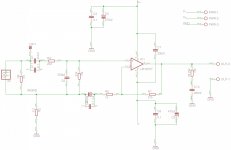
I believe i might have a solution to the loop problem Andrew pointed out. R2 needs some repositioning.
What diameter is the C4? I think a 8mm cap sould cover most of the needs there.
It could be moved closer to the board top edge.
C11 on the top side of C1.
With those changes you should be able to move the R2 upwards and have the loop smaller.
What diameter is the C4? I think a 8mm cap sould cover most of the needs there.
It could be moved closer to the board top edge.
C11 on the top side of C1.
With those changes you should be able to move the R2 upwards and have the loop smaller.
Excellent!
And now you move the input ground connection from the C4 to the R2 top pin.
Then the connection between R2 and C4 as thick as possible.
If that wont make the loop as small as possible, i do not know what will...
Next step, the power park...
You have a choise to make.
The red pill or the blue pill.
With the red pill we stick to the current layout, only make some minor adjustments.
But with the blue pill i will (try to) take you to a place with no turning back. Completely rearrange the power and the output.
I have reduced it from 13mm to 10.5mm. Please let me know if I should reduce it further to 8mm. I can reduce the value also, as its currently 220uf, probably 47uf should do here ok. Whats the max voltage that this cap will see.
Voltage rating for C4 is as low as +/-2V. A 6,3 to 10V cap OK.
220uF 6.3V BiPolar is 8mm. However your 10mm dia cap seems to fit in there quite nicely.
- Status
- Not open for further replies.
- Home
- Amplifiers
- Chip Amps
- please review this pcb design