Hi All.
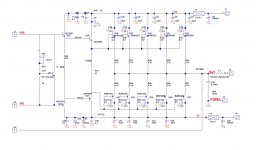
I have been very busy on the IPS VAS design. I am coming back to the OPS board. I decided to remove the error correction as I have no plan to use MOSFET. Here is my latest schematic. I want to look into using the extra space to put in the SS relay to protect the speaker.
My question is whether there is any advantage to replace the NPN(Q20) predriver with PNP and PNP( Q21) with NPN?
If so, can anyone give me a proven circuit to replace the transistors? In Cordell, he need CCS if you try to use the opposite transistor. I know people have circuit that does not need that. I just want a proven design.
Also, any suggestion to improve this OPS?
Thanks
Attachments
This circuit is very similar to, but not as good as, OStripper's SlewMaster OPS...
Might I suggest you copy that, or better yet, source some of his beautifully laid out boards, and with the time saved spend it on the more interesting aspect; the input stage.
But failing that my advice would be:
- Put the adjustment pot into the B-E junction of the Vbe transistor so that when it goes open wiper the failure mode is not catastrophic.
- You need more gain in the bias generator if you want to play with push-pull VAS designs.
- Are the driver, pre-driver, and output transistors mounted on separate heatsinks? You will need to think about how to sense the tempco's of these different stages.
- I think your driver transistors are a little lightweight considering the number of outputs. Consider using another output device as driver stage.
- Add zobels to the B-C junctions with the fc calculated to suit the device characteristics. This will help improve stability in 3EF topology.
- You might need to increase the OP Rb to 3R3 or 4R7
- Increase the OP Re to 0R22 and be prepared to increase it further subject to device variation
Thanks- Put the adjustment pot into the B-E junction of the Vbe transistor so that when it goes open wiper the failure mode is not catastrophic.
- You need more gain in the bias generator if you want to play with push-pull VAS designs.
- Are the driver, pre-driver, and output transistors mounted on separate heatsinks? You will need to think about how to sense the tempco's of these different stages.
- I think your driver transistors are a little lightweight considering the number of outputs. Consider using another output device as driver stage.
- Add zobels to the B-C junctions with the fc calculated to suit the device characteristics. This will help improve stability in 3EF topology.
- You might need to increase the OP Rb to 3R3 or 4R7
- Increase the OP Re to 0R22 and be prepared to increase it further subject to device variation
I am thinking about the bias generator. I like yours with a PNP sourcing the current when the current through the collector of the NPN is over 0.7mA ( dropping 0.7V across the 1K resistor). But my question is should I lower the resistor to get say 5mA through the NPN before turning on the PNP? Say using a 200ohm resistor at the collector instead of 1K?
Is it only the NPN of the bias generator mounted on the heat sink, the PNP is of no importance, any small signal like BC556 will do?
I have done a lot of RF and microwave pcb layout. I am using ground plane and power plane for the power transistors and the pre-drivers. I have 0.1u ceramic cap right on the collector of each transistor to ground that should be good enough for RF circuit. I have 10uF for most of the transistors from collector to ground also. Too bad I don't know how to copy the layout into JPG file to post. I think I have a very good layout that can support tens of MHz circuit. All base resistors are point to point to the base lead of the transistors. If I need zobel network ( lag lead), I'll solder right on the pins of the transistor.
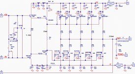
I increased the base stop resistors and move the adjustment pot.
Thanks
Attachments
Last edited:
I see you moved tpot1 to the BE side of the multiplier.
Your minimum multiplier ratio is too high.
{4k99/(200+909)}+1 = 5.5Times Vbe, decrease R68 a lot. (or use 2k for Tpot).
The maximum multiplier ratio is about right, if the output stage Vbe are similar to the multiplier Vbe.
{4k99/0k909} + 1 = 6.49times Vbe
I would reduce R71, 909r, a lot and increase Tpot a lot.
The pre-driver and driver bias currents shown will only be achieved if you set the output devices so high they blow up.
If you want these two currents (5.6mA & 28mA) you will need to reduce R62 & R61 a bit, maybe to around 84%.
You may find that the base stopper values are a bit high. They are around the maximum you would use in these locations.
Try making them as small as allows the amp to maintain the stability margins you have set for yourself.
Add a damping resistor across L1
Maybe allow pads for adding Ccb across all the pre-drivers and drivers.
What does F indicate on the Power Grounds?
Your minimum multiplier ratio is too high.
{4k99/(200+909)}+1 = 5.5Times Vbe, decrease R68 a lot. (or use 2k for Tpot).
The maximum multiplier ratio is about right, if the output stage Vbe are similar to the multiplier Vbe.
{4k99/0k909} + 1 = 6.49times Vbe
I would reduce R71, 909r, a lot and increase Tpot a lot.
The pre-driver and driver bias currents shown will only be achieved if you set the output devices so high they blow up.
If you want these two currents (5.6mA & 28mA) you will need to reduce R62 & R61 a bit, maybe to around 84%.
You may find that the base stopper values are a bit high. They are around the maximum you would use in these locations.
Try making them as small as allows the amp to maintain the stability margins you have set for yourself.
Add a damping resistor across L1
Maybe allow pads for adding Ccb across all the pre-drivers and drivers.
Maybe allow space to increase the output decoupling >>10uF, upto 1mF ?Add zobels to the B-C junctions with the fc calculated to suit the device characteristics.
What does F indicate on the Power Grounds?
Last edited:
Ranchu,
I am working on a different amp and the margins seem to be so low that small changes make the amp oscillate.
How do you go about predicting what R+C is required across the CB junctions?Add zobels to the B-C junctions with the fc calculated to suit the device characteristics.
I am working on a different amp and the margins seem to be so low that small changes make the amp oscillate.
Ranchu,
How do you go about predicting what R+C is required across the CB junctions?
I am working on a different amp and the margins seem to be so low that small changes make the amp oscillate.
Hi Andrew,
The only real way I can see to workout the values of R+C is to analyse that loop. Preferably using the Tian probe method.
Paul
Hi Andrew
My rule of thumb, which has proven to be reliable for me in this specific context, is to set the R+C to about 50% of the device's bandwidth product, up to a maximum of about 30-50Mhz, allowing for PC board parasitics.
I have found that adding these zobels to either the driver or output stages, is one of the most effective ways to achieve an utterly stable EF3. Of course proper PC board layout and rail decoupling is also crucial, but I am finding that the zobel network is so effective that the usual Rb requirements can be relaxed somewhat.
Don't want to stray too far off, so I intend doing an .asc in another Thread and asking for help.Hi Andrew,
The only real way I can see to workout the values of R+C is to analyse that loop. Preferably using the Tian probe method.
Paul
But some of what has been discussed so far is applicable to Alan's implementation.
I am trying to make the trim pot less sensitive, only from 5.5 times to 6.5 times. That should cover the range of adjustment. Max bias current is when the trim pot is zero so the Vbe multiplier is about 6.5 times. I thought this would be the best.I see you moved tpot1 to the BE side of the multiplier.
Your minimum multiplier ratio is too high.
{4k99/(200+909)}+1 = 5.5Times Vbe, decrease R68 a lot. (or use 2k for Tpot).
The maximum multiplier ratio is about right, if the output stage Vbe are similar to the multiplier Vbe.
{4k99/0k909} + 1 = 6.49times Vbe
I would reduce R71, 909r, a lot and increase Tpot a lot.
Yes, I'll do that.Add a damping resistor across L1
I do have 1mF on the other side of the fuse for each rail. The symbol of the cap is very small like the normal 10uF. I want to keep it on the other side of the fuse to avoid blowing the fuse during power on charging up. I have 10uF from to collector to ground of 4 out of 5 transistors to cover the local current return. They are close to point to point from collector to ground ( about 1/4" max). As I describe, there will be a ground and power planes where the transistors are, so there is no trace inductance to talk about. The base stop resistor is point to point (1/8") from the base pins of all the transistors.Maybe allow pads for adding Ccb across all the pre-drivers and drivers.
Maybe allow space to increase the output decoupling >>10uF, upto 1mF ?
What does F indicate on the Power Grounds?
Each transistor has a 0.1uF ceramic cap within 1/8" from the collector pin straight to the ground plane. This is good for 100MHz design. The collector of each transistor literally have a 10uF parallel with 0.1uF capacitor bypassed to ground plane. Then a 1000uF as reservoir. I never deal with high power transistor before. For small signal, this scheme should be solid unless the fT of the transistor is over 1GHz. Then I might need ferrite beats on the collector pin.
The "F" ground is just a name, nothing more.
Thanks
Last edited:
IMHO
A lot of the parasitic oscillation of transistors mainly due to the lack of ground plane and power plane. from my experience, transistor that has fT under 700MHz is quite stable, you have to make them oscillate. It only gets dicey when you are dealing with the one over 1.5GHz. In audio amps, all too often, I see ground trace and power trace are running around to tide to transistors. The traces present as both inductors and worst is forcing current to run on specific path that cause voltage drop along the line. If you have ground and power line going from one transistor to another, you literally feed signal from the collector of one transistor to the other.
That's the reason I started the layout on the premises of having a full ground plane and power plane on all the transistors. Layout stacking is where the battle won or lost. I spent a lot of time looking at the ground plane and power plane to make sure they don't get cut up accidentally by the pads being too close. It has to be a continuous plane. It's one thing to design the circuit, but a lot of engineers lost their battle because of a bad layout.
I even have a partial plane for the output rail, I don't have ground plane under the output plane to avoid capacitance from output to ground. More important, I don't want the output signal to inject current onto the ground plane.
BTW:
I just bought this chassis:4015 Class A Amplifier Aluminum Chassis CPI Chassis After Enclosure | eBay
Now I am waiting for the axe to fall on my head from my big boss!!!😱😀 I need to have my hands on the chassis, measure the spacing of the fins to finalize the pcb of the OPS. I want to make sure I drill holes for the transistors at the right place and make sure I can fit both the OPS board and the IPS/VAS board all on the heat sink.
Last edited:
I forgot to ask, Should I get a beefier driver transistor( second EF driving all the big transistors). It's a lot of capacitance to drive. I read recommendation of MJE15032/15033. My issue is fT of 30MHz only and low beta.
I forgot to ask, Should I get a beefier driver transistor( second EF driving all the big transistors). It's a lot of capacitance to drive. I read recommendation of MJE15032/15033. My issue is fT of 30MHz only and low beta.
I don't like the MJE15032/33 either. Too slow. I use the C5171/A1930 transistors myself but your choice is good / better. IMHO, it would be better to parallel another pair of the same than change to those MJEs.
Hi Alan, interesting comments. I will be most interested to see what layout you come up with.
I have to find a way to transfer the layout into jpg file.
This is the best I can do so far. I have to put it in pdf file. Because of the limitation of the display, I have to create 4 files. 1) components and routes. 2) components and ground plane. 3) components, output plane and power planes. And finally the complete file with both planes, components and routes. I cut off the two ends so I can show more details. The file only show about 3 stages instead of 5.
This is the old file with the error correction that I decided to get rid of. But you'll see my idea. Use the 1) to see the component placements, use the 4) to see with the planes.
Part of the reason I get rid of the error correction is because it makes too many holes on the ground plane. As you can see, even after I carefully place the components to avoid a long cutting on the ground plane (see second file), it still looks like a Swiss cheese.
Notice I have 0.1u ceramic cap right next to the collector of all the transistors? then the 10uF close by. All connect from power plane to ground plane. The power and ground plane should behave like a one solid plane. I try to avoid plane under the base drive trace as much as possible. I also avoid the output plane over the ground plane as much as possible. This one is hard as the error circuit cut up the ground plane too much and I have to extend the ground plane up. The new version without the error circuit will be a lot better.
Attachments
Last edited:
There are Sanken 125w to-3p's at 60mhz Ft and <110Cob -
edit - 2sa1186 / 2sc2837
Many other Sanken "LAPD" MT-100's >35mhz Ft <200Cob at higher Vceo.
way better and badder than the MJE's for a hefty EF3.
Ground plane for an OPS ??
OS
edit - 2sa1186 / 2sc2837
Many other Sanken "LAPD" MT-100's >35mhz Ft <200Cob at higher Vceo.
way better and badder than the MJE's for a hefty EF3.
Ground plane for an OPS ??
OS
Those two are good!!! You mean to use it as drivers right? Thanks.There are Sanken 125w to-3p's at 60mhz Ft and <110Cob -
edit - 2sa1186 / 2sc2837
Many other Sanken "LAPD" MT-100's >35mhz Ft <200Cob at higher Vceo.
way better and badder than the MJE's for a hefty EF3.
Ground plane for an OPS ??
OS
Yes, I use ground plane for all the boards. Seen way too many problems with layout in my lives. Still 2 layers, just more work on me, not costing anything more. Designing circuit is one thing, to me, it's the easy thing. Make it not oscillate is the real battle in a lot of circuits. Even though 500KHz is low frequency, problem with OPS is the circuit spread out, traces make long run because of the size of the components. You can't say just because it's only 500KHz and it's all good. Also, the amount of current going through the traces can make it do funny things.
Last edited:
About ground planes in high current areas. You will see symmetric , short loop
paths and those current returns confined to certain areas of a layout.
Paths are high current and short from decoupling to main ground (PCB star).
They will actually cancel at this physical point.
Many amp layouts on the forum will bring both grounds and individual rails
all the way around the circumference of a large PCB , all that return current
produced by decoupling and the outputs has a long way to return to a common
ground. Any small signal component close is inductively coupled by proximity.
A separate "dirty ground" / "clean ground" is a step in the right direction.
Badger and slewmaster are all G1/G2 based (just look at the posted layouts).
High current on a ground plane is unpredictable , unless you were to split the plane
+/- and have it channeled to the star. Still , it would be like a big "radiator" for
rail "garbage" until it converged at the star.
RF/low current is a whole different matter (PC mainboards -mobile). We filter
this out of our amps at the PS and input.
Edit - the amp should not produce this , regardless ... so it is not a concern.
Examples are the DIYA store badger - like an ADCOM GFA series amp
NO ground planes there. Or , my slewmaster with a harmon Kardon style
OPS.
BOTH are dead silent - NO hum , no oscillation - just music.
OS
ditto on the gnd deal. Since it is the smoothing caps (not the filter caps which should be separated by a small R or RL on the rails [C-R-C-C-c]), it is important to keep the return currents of the first filter caps (dirty gnd) separate from the smoothing cap bank center point return (star gnd). Signal gnd is separate from this point as well. Poor grounding can lead to all kinds of problems.
 😛
😛
😛
Last edited:
If you look at my layout carefully, you'll find the main 1000uF filter cap is at the upper part of the ground plane away from the power transistor. That is the one needs to be far from the amp part. They are before the fuse and the main power plane. The FGND pick up point is at the upper part of the plane. The big ripple current is guided away from the transistors. The ground plane in the transistor area is too ensure no trace inductance, no parasitic.About ground planes in high current areas. You will see symmetric , short loop
paths and those current returns confined to certain areas of a layout.
Paths are high current and short from decoupling to main ground (PCB star).
They will actually cancel at this physical point.
Many amp layouts on the forum will bring both grounds and individual rails
all the way around the circumference of a large PCB , all that return current
produced by decoupling and the outputs has a long way to return to a common
ground. Any small signal component close is inductively coupled by proximity.
A separate "dirty ground" / "clean ground" is a step in the right direction.
Badger and slewmaster are all G1/G2 based (just look at the posted layouts).
High current on a ground plane is unpredictable , unless you were to split the plane
+/- and have it channeled to the star. Still , it would be like a big "radiator" for
rail "garbage" until it converged at the star.
RF/low current is a whole different matter (PC mainboards -mobile). We filter
this out of our amps at the PS and input.
Edit - the amp should not produce this , regardless ... so it is not a concern.
Examples are the DIYA store badger - like an ADCOM GFA series amp
NO ground planes there. Or , my slewmaster with a harmon Kardon style
OPS.
BOTH are dead silent - NO hum , no oscillation - just music.
OS
I worked many years in signal integrity and layout. I never ever once run into problem. People try to out smart the ground and power will run into trouble sooner or later. This has been argued over and over and there is no point to hash it again.
Last edited:
- Status
- Not open for further replies.
- Home
- Amplifiers
- Solid State
- Please comment on my OPS design