I don't know what exactly is your arrangement but have you tried something like this?
In general, a Baker clamp is a circuit that avoids transistor staturation. In audio, a Baker clamp is usually wrapped around the VAS transistor(s), avoiding their saturation and hence avoiding the ugly transient response (since the loop gain collapses and the recovery from saturation is rather slow for bipolars), when the amplifier input is overdriven.
The diodes in your schematic have the role to avoid the emitter follower saturation due to the possible excess voltage from the VAS output. That's the diode clamping I was talking above in #407, to avoid the VAS output to exceed the output stage power supply voltage. So while the circuit is technically a Baker clamp (in the generic sense) it does not play the role of clipping protection, as usual in audio amplifiers, but more like avoiding the amplifier to self destruct.
It is true that a Baker clamp has an impact on the circuit distortions, because a nonlinear capacitance (the diodes) is added, and the reverse bias voltage swing is rather large. This can be avoided by bootstrapping the Baker clamp, making the diodes to have a rather constant reverse bias voltage.
Last edited:
Hi Ovidiu (if you allow me to call you this way),
Of course you're right about the purpose of the Baker clamp and this is well known. The idea in schematic I proposed is not mine - it's an excerpt from a well know book which I happen to find circulating the Web (actually I believe that "If we can see further it is because we stand on the shoulders of giants").
Of course I know there are an additional measures which can be taken for clipping protection - in particular your very interesting and unusual input stage described here: YAP Front End
My point was that if Трифон (the Cyrillic transcription of the name Tryphon - yes, we happen to have the same name used) wants to use a raised Input stage power supply, he has an easier way to implement the Baker clamp not raising the number of active devices he tries to avoid.
Well this not means it can avoid the presence of non-linear p-n junction capacitances so if you introduce your idea for bootstrapped clamp it will be interesting (at least for me).
Regards
Alex
Exactly.I don't know what exactly is your arrangement but have you tried something like this?
Of course I know there are an additional measures which can be taken for clipping protection - in particular your very interesting and unusual input stage described here: YAP Front End
The YAP front end clipping protection schematic is a very good example of bootstrapping a diode clamp; the idea is to drive the other end of the diode with a slightly level shifted copy of the variable signal (here: the VAS output). This makes the reverse bias of the protection diodes approximately constant (in the range where the clamp is inactive) so that the reverse bias ed diode capacitance is rather constant, so no extra distortions are created.
There is no universal recipe for bootstrapping, and I don't see any trivial/simple way to bootstrap the follower saturation Baker clamp you posted above.
As far as I'm concerned, it's likely.What happen to this thread? Is it permanently locked?
One reaps what one sows.
For those who are interested by this amp's evolution: feel free to PM me.
Attachments

Last edited:
And, as a gift of departure from this forum, like so many before me for the same reasons, the finished version of the Pizzicato V 250W amplifier.
Need a 75V regulated supply for the front end. (<100mA)
Great care has been took on important details, like rail sticking, ability to afford huge clipping with no time limitation. (despite the protection will not allow-it). This comes at the price of a little reduced performance in distortion. But they still look good enough ;-)
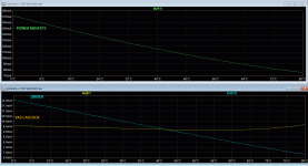
0.000001% à 1W 8Ohms 1000Hz
0.000009% @100W
0.000013% à250W
>100dB loop gain.
Of course, they will, for sure, be not so impressive in real world, but I'm confident they will be lot, lot under any audibility threshold.
Great care has been took on the VAS tempco as well. Current is very stable all over the temperatures), decreasing with temp everywhere else.
Of course, it is just simulations and we will see how this amp will behave and sound on the bench, but I'm pretty confident that it will require only little adjustements.
This was part of the game, to explore if it is possible to design an amp only with a simulator and have-it working on the Bench. The opposite of my usual way.
Krisfr, this is the final version, no more change before the first builds (I apologize for all those previous ones).
I will stay on your side, here, for your printed board evolution.
I want to thank-you, and thank all the nice people that had participated to this project, and helped with their suggestions and advice, specially spladski and Dimitri.
Will make no comment about the aggressivity of some others. Some seems good engineers, but poor human being: Life is too short to loose time with such individuals. I was here to meet new friends, share our experiences and little knowledges (it is only Hifi), spend nice time in friendly exchanges. Not the right place, obviously.
For those who are interested in building this amp, feel-free to PM me, I will be on your side as much as I can.
Need a 75V regulated supply for the front end. (<100mA)
Great care has been took on important details, like rail sticking, ability to afford huge clipping with no time limitation. (despite the protection will not allow-it). This comes at the price of a little reduced performance in distortion. But they still look good enough ;-)
0.000001% à 1W 8Ohms 1000Hz
0.000009% @100W
0.000013% à250W
>100dB loop gain.
Of course, they will, for sure, be not so impressive in real world, but I'm confident they will be lot, lot under any audibility threshold.
Great care has been took on the VAS tempco as well. Current is very stable all over the temperatures), decreasing with temp everywhere else.
Of course, it is just simulations and we will see how this amp will behave and sound on the bench, but I'm pretty confident that it will require only little adjustements.
This was part of the game, to explore if it is possible to design an amp only with a simulator and have-it working on the Bench. The opposite of my usual way.
Krisfr, this is the final version, no more change before the first builds (I apologize for all those previous ones).
I will stay on your side, here, for your printed board evolution.
I want to thank-you, and thank all the nice people that had participated to this project, and helped with their suggestions and advice, specially spladski and Dimitri.
Will make no comment about the aggressivity of some others. Some seems good engineers, but poor human being: Life is too short to loose time with such individuals. I was here to meet new friends, share our experiences and little knowledges (it is only Hifi), spend nice time in friendly exchanges. Not the right place, obviously.
For those who are interested in building this amp, feel-free to PM me, I will be on your side as much as I can.
Attachments
-
pizzicato-v 250-def.asc46.7 KB · Views: 161
-
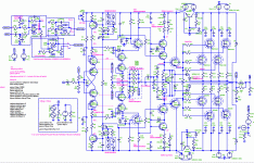 pizzi-schema.gif97.7 KB · Views: 2,827
 -
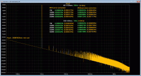 pizzi-def-disto.gif90.6 KB · Views: 2,235
 -
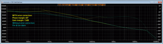 Pizzi-def-loop.gif39.6 KB · Views: 591
 -
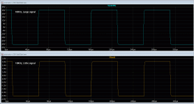 pîzzi-def-square.gif37.1 KB · Views: 550
 -
 Pizzii-def-response curve.gif34.3 KB · Views: 170
 -
 Pizzi-def-clipping.gif110.2 KB · Views: 172
 -
 Pizzi-def-tempco.gif37.8 KB · Views: 234

The protection schematic is in Post 378.
Soft start, remote, silent stop, temperature and fans (if needed) monitoring etc.
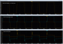
Fires in case of clipping, short circuit of output wires, DC in input or output, and any amp oscillations in less than 25µs.
It is a modified version of the protection published by Esperado in this thread:
An ultimate amp protection circuit ?
Soft start, remote, silent stop, temperature and fans (if needed) monitoring etc.
Fires in case of clipping, short circuit of output wires, DC in input or output, and any amp oscillations in less than 25µs.
It is a modified version of the protection published by Esperado in this thread:
An ultimate amp protection circuit ?
Last edited:
Honestly it would be a (very pleasant!) surprise to see any photos of completed, debugged, chassis-mounted, working Pizzicato_200W amplifiers.
The design uses 4 complementary pairs of unobtanium TO3 output devices, which sell on eBay for USD 19 per pair (link to example) and the buyer has no assurance the parts are genuine or reliable. I doubt that many DIYers will invest the necessary resources, including their own time, in such a project. But I hope someone proves me wrong.
The design uses 4 complementary pairs of unobtanium TO3 output devices, which sell on eBay for USD 19 per pair (link to example) and the buyer has no assurance the parts are genuine or reliable. I doubt that many DIYers will invest the necessary resources, including their own time, in such a project. But I hope someone proves me wrong.
Some explanations of our final choices.
The strange arrangement of the input stage was motivated by the need of VBE match of the input active devices.
We have chosen (brilliant spladski's idea) to use CIs (pairs of matched transistors).
Using one of them in the first stage of the input stage as an active device, and the other as a diode in the second stage (and the contrary). This avoid any need to match them on the bench (they are VBE matched in the CI), and let them closely coupled on temperature changes. The first and second stages of the input part compensate each other.
This was needed by our desire to set a maximal gain in the input stage (No degeneration).
And by the fact that all the quiescent currents of the amp are set by the CSS of the first stage.
As the power dissipation of those pairs was not high enough, a cascode was finally needed (Again a spladski's idea), that brings some benefits on the HF response and distortion as well.
The strange arrangement on the current sources was my effort to get a tempco that pre-compensate as well as possible the VAS tempco. The result is quite flat in VAS simulations: we will see if it matches in real life, but there is enough room in the schematic to allow some tweaks IRL without any expected need to modify the printed board if any need.
The Schottky diodes around some transistors are used to clamp them in case of hard clipping and avoid rail sticking, all along with the choices of the base voltages of the input and VAS Cascodes to limit the max currents.
The diodes that protect output devices from dangerous gate/sources voltages was moved to the VAS stage, to protect the driver transistor for excess of current if it happens. Idea from Bob Cordell, suggestion of some members. Thanks to them.
Reverse diodes (thanks Dimitri) in the output stage to protect the power devices from any accident due to inductive loads.
Stabilized PSU for Input and VAS stage were chosen for two reasons. First, there is a 5V losse in the MOSFETS. Second, CFA input stages don't offer a so good ripple rejection than Long Tailed pairs at low frequencies. This will address the two issues.
Care has been taken to don't drive them too close to their saturation point if the 5V difference is respected. But this is not critical.
Last, we use a output stage inclusive compensation schematic. The benefit, compared to the classical miller cap is a noticeable improvement in distortion.
In a pretty strange way ?
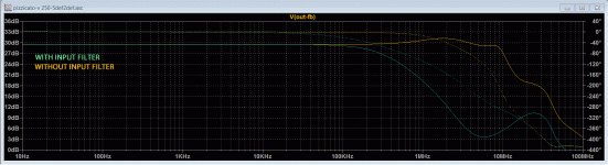
This is motivated by the desire to use the same printed board for an other more classical CFA version "C", with less open loop gain, flat OLG up to 10KHz, classical TMC. With a little added improvement on this future version following Dadod's Idea (VAS emitter network). Not used in this VFA version because degeneration resistance is too low to let an usable margin but visible on the schematic.
The Integrated circuits in the schematic are used for several purposes. Optional error correction, that add some 10dB more feedback to the amp, DC servo used in an original way, and, while we are here, protection.
The theory of operation is simple: we subtract the original signal from the output one, keeping (in theory ;-) only the differences (distortion and DC shifts).
For the DC servo, this will reduce sonic signature (if any) of the integrated circuits, because the musical signal has been removed before DC compensation is applied.
I think it will be the same with error correction. Not to forget that, once the original signal is removed by the comparator of the (fast) input stage of the first IC, the signal levels in the integrated circuits are highly reduced, as well as the distortions that comes with-it.
Too the phase response of the error correction was set in a way that allows the same amp to work both with error correction and without, keeping phase and gain margins at HF unchanged. Trying to get-it effective enough in the all audible frequency range. We will see on the bench if this can be improved at 20KHz without compromising stability.
The strange arrangement of the input stage was motivated by the need of VBE match of the input active devices.
We have chosen (brilliant spladski's idea) to use CIs (pairs of matched transistors).
Using one of them in the first stage of the input stage as an active device, and the other as a diode in the second stage (and the contrary). This avoid any need to match them on the bench (they are VBE matched in the CI), and let them closely coupled on temperature changes. The first and second stages of the input part compensate each other.
This was needed by our desire to set a maximal gain in the input stage (No degeneration).
And by the fact that all the quiescent currents of the amp are set by the CSS of the first stage.
As the power dissipation of those pairs was not high enough, a cascode was finally needed (Again a spladski's idea), that brings some benefits on the HF response and distortion as well.
The strange arrangement on the current sources was my effort to get a tempco that pre-compensate as well as possible the VAS tempco. The result is quite flat in VAS simulations: we will see if it matches in real life, but there is enough room in the schematic to allow some tweaks IRL without any expected need to modify the printed board if any need.
The Schottky diodes around some transistors are used to clamp them in case of hard clipping and avoid rail sticking, all along with the choices of the base voltages of the input and VAS Cascodes to limit the max currents.
The diodes that protect output devices from dangerous gate/sources voltages was moved to the VAS stage, to protect the driver transistor for excess of current if it happens. Idea from Bob Cordell, suggestion of some members. Thanks to them.
Reverse diodes (thanks Dimitri) in the output stage to protect the power devices from any accident due to inductive loads.
Stabilized PSU for Input and VAS stage were chosen for two reasons. First, there is a 5V losse in the MOSFETS. Second, CFA input stages don't offer a so good ripple rejection than Long Tailed pairs at low frequencies. This will address the two issues.
Care has been taken to don't drive them too close to their saturation point if the 5V difference is respected. But this is not critical.
Last, we use a output stage inclusive compensation schematic. The benefit, compared to the classical miller cap is a noticeable improvement in distortion.
In a pretty strange way ?
This is motivated by the desire to use the same printed board for an other more classical CFA version "C", with less open loop gain, flat OLG up to 10KHz, classical TMC. With a little added improvement on this future version following Dadod's Idea (VAS emitter network). Not used in this VFA version because degeneration resistance is too low to let an usable margin but visible on the schematic.
The Integrated circuits in the schematic are used for several purposes. Optional error correction, that add some 10dB more feedback to the amp, DC servo used in an original way, and, while we are here, protection.
The theory of operation is simple: we subtract the original signal from the output one, keeping (in theory ;-) only the differences (distortion and DC shifts).
For the DC servo, this will reduce sonic signature (if any) of the integrated circuits, because the musical signal has been removed before DC compensation is applied.
I think it will be the same with error correction. Not to forget that, once the original signal is removed by the comparator of the (fast) input stage of the first IC, the signal levels in the integrated circuits are highly reduced, as well as the distortions that comes with-it.
Too the phase response of the error correction was set in a way that allows the same amp to work both with error correction and without, keeping phase and gain margins at HF unchanged. Trying to get-it effective enough in the all audible frequency range. We will see on the bench if this can be improved at 20KHz without compromising stability.
Last edited:
Honestly it would be a (very pleasant!) surprise to see any photos of completed, debugged, chassis-mounted, working Pizzicato_200W amplifiers.
The design uses 4 complementary pairs of unobtanium TO3 output devices, which sell on eBay for USD 19 per pair (link to example) and the buyer has no assurance the parts are genuine or reliable. I doubt that many DIYers will invest the necessary resources, including their own time, in such a project. But I hope someone proves me wrong.
You can buy TO3 laterals here Lateral MOSFETs | Profusion
The Ebay lister seems to have 100% satisfaction rating and been there for 18 years. HIS reputation seems to be reputable...
Are the Exicon devices interchangeable with the originals 134 & 149?
Are the Exicon devices interchangeable with the originals 134 & 149?
The POWER MOSFETS noted on the schematic are just here to can use the Cordell models I had during the simulation. And you will notice that they are not even the correct ones (Drain source max voltage) that should be: 2SK135, 2SJ50.The Ebay lister seems to have 100% satisfaction rating and been there for 18 years. HIS reputation seems to be reputable...
Are the Exicon devices interchangeable with the originals 134 & 149?
I thought it was obvious.
Any convenient modern laterals (power and DSV) will do the job, including double die Renesas to replace a pair. TO3 is just an option for those that still have some of them left.
The components used here are just indicative and i'm sure that a lot of DIYers here have a lot more experience on this than me, that was far from amp design those last decades.
Of course, we will do the final BOM together and , as I said, i'm am here to answer YOUR questions and work on your side (as well as questions from others, more interested by this amp than just trying to discredit this work by any possible means ;-)
Any suggestions will be welcomed.
By the way, the MMBD5004BRM noted by mistake in comment in the schema will be better replaced by a simple set of 4 X IN4148. Those 1N4148 were the ones used in the simulation and will have, I think, better coupling with ambient temperature. .
Last edited:
Thanks for your nice encouragements and so judicious remarks.Honestly it would be a (very pleasant!) surprise to see any photos of completed, debugged, chassis-mounted, working Pizzicato_200W amplifiers.
The design uses 4 complementary pairs of unobtanium TO3 output devices, which sell on eBay for USD 19 per pair (link to example) and the buyer has no assurance the parts are genuine or reliable. I doubt that many DIYers will invest the necessary resources, including their own time, in such a project. But I hope someone proves me wrong.
It is obvious any complementary pair of lateral Mosfets of >= 125W and drain source voltage >= 160V will fit. TO-3 as well as TO-264.
Of course, the Exicons.
Or, by example, the double die Renesas pairs:
2SK1058 2SJ162 (A little limit in voltage (160V max)
2SK2220 2SJ 351
2SK2221 2SJ352
(Only need to use 2 power devices instead of 4 for each 1/channel.)
Or EMLAB ALF16N20W - ALF16N20W (Only need too)
Or ALFET ACD101NDD and ACD103PDD (Only need too) etc...
Last edited:
Found those interesting comments of our respected member vzaichenko about error correction:
No-global-loop amplification
No-global-loop amplification
Welcome back Professor! I was a bit afraid that you would do what you said, leave and not come back! Luckily you reconsidered.
Yes indeed, V's amp is quite interesting! As I noted in that thread, it reminded me of my own adventures with ODF and error correction. At the time I was so young and naïve that I spend a lot of money on a patent that later turned out to be worthless.
Ahh, we live and learn!
Jan
Yes indeed, V's amp is quite interesting! As I noted in that thread, it reminded me of my own adventures with ODF and error correction. At the time I was so young and naïve that I spend a lot of money on a patent that later turned out to be worthless.
Ahh, we live and learn!
Jan
Welcome back Professor! I was a bit afraid that you would do what you said, leave and not come back! Luckily you reconsidered.
Yes indeed, V's amp is quite interesting! As I noted in that thread, it reminded me of my own adventures with ODF and error correction. At the time I was so young and naïve that I spend a lot of money on a patent that later turned out to be worthless.
Ahh, we live and learn!
No, i have not reconsidered. I will leave the forum when this project will be achieved. Disgusted by the aggressive ambiance. And I think the moderation team is greatly responsible of it.
Yes, I had read your adventures with "ODF", similar to mines (apart Patent attempts ;-)
My experiences (similar to the one of another member of the forum) was if it changes the measured numbers, it do not have so much impact on the character of an amp when not in action, comparing listening experiences. What is your point of view and experiences about this point ?
By the way, I think my attempt for a collaborative design was in a way not a success, and, for sure, I am responsible of it, despite my tries to play more naive or unwashed than I am ;-) in order to let max doors opened.
My desire was too to allow lurkers to discover across exchanges some dev important points, discussing together all the details, their consequences and various ways to address them (tempco, VBE missmatches etc.).
I regret that most of the valuable remarks has been made in the form of criticisms rather than suggestions.
I reacted on their form, not on their validity. My mistake., but friendship and cool atmosphere are more important for me than any technical correctness.
As you can see, thanks to some very good suggestions, the final design respect totally the initial intentions, respecting the base schematic, and, as far I can imagine, all the points that needed to be addressed (obvious to me since the beginning)...had been addressed ... in a elegant way ?
I still need suggestions on some points, and returns of experiences, like ... base stoppers in Cascodes ?
I'm very curious to build and listen to this amp, that is the opposite of everything in which I believed since now. I am sure i will learn a lot of things and, may-be, have to reconsider many of my believes. Strangely, at the end, this amp smell good to me ;-)
Last edited:
No, i have not reconsidered. I will leave the forum when this project will be achieved.
I doubt it. I think you like/need the attention. If you hate it here so much, why not leave right now then? You can finish your amp in the closed circle of your buddies, you don't need the forum for that.
Mind you, I think you should stay!
Jan
Your efforts to be gentle or even simply polite do not last long.I think you like/need the attention.
Last edited:
- Home
- Amplifiers
- Solid State
- Pizzicato, a 200W low distortion CFA amplifier