ok, for the transistor - take the ohm-meter, if there is a special mode for testing the diodes - use that one, otherwise set the range to let say, 1 MOhm.
First check resistance between collector and emitter - must be infinity both directions.
Then connect one of the probes to the base and check collector and then emitter with the other one. Then change the probe at the base and do the same. Base-collector and base-emitter must show some resistance in one direction. In the other direction - infinity.
If there is low measurement somewhere - transistor is shortened inside. If there is no resistance in both directions from the base - it is broken (cut to infinity).
C20 reads 4.8 µF (spec is 4.7)
OK, I guess Q4 must be broken as well:
Neg to left Pos to ctr: 0.0545V
Neg to left Pos to Right: 0.0538V
Neg to ctr Pos to left: 0.0556V
Neg to ctr Pos to Right: 0.0024V
Neg to Right Pos to left: 0.0540V
Neg to Right Pos to ctrt: 0.0027V
10 ten years ago I had the power supply assy fixed after serious overheat, and then changed Q4. I have kept the original B682 that was there at the time and it checks out what in my limited world seems normal to 0.59.
Since I do not have other replacements at hand I would like your opinon as to put it back in?
Yes, Q4 is definitely shortened (bricked)...
I think, if the original one looks good (try to check it the way I mentioned above), then it will be ok to put it back in.
The question is - what made the previous Q4 shorten... overheat? because of overload?
Is there some heat-sink on Q4?
I think, if the original one looks good (try to check it the way I mentioned above), then it will be ok to put it back in.
The question is - what made the previous Q4 shorten... overheat? because of overload?
Is there some heat-sink on Q4?
Last edited:
ok, for the transistor - take the ohm-meter, if there is a special mode for testing the diodes - use that one, otherwise set the range to let say, 1 MOhm.
First check resistance between collector and emitter - must be infinity both directions.
Then connect one of the probes to the base and check collector and then emitter with the other one. Then change the probe at the base and do the same. Base-collector and base-emitter must show some resistance in one direction. In the other direction - infinity.
If there is low measurement somewhere - transistor is shortened inside. If there is no resistance in both directions from the base - it is broken (cut to infinity).
My problem is that I never seem to understand exactly where e-b-c pins are. I have looked at a spec sheet for one of the trannys I purchased for this project, and from the depiction in the datasheet: http://www.fairchildsemi.com/ds/KS/KSA1381.pdf
I would place the trans (PNP - Pos-Neg-Pos) with the fine type print up (readable), lead pointing i my direction I would have emitter to the left, collector in center and base to the right:
Do I want to connect my red test probe to 1 (e), and test 2 (c) and 3 (b) with the black testprobe?
That gives me OL (out of limits) and 0.68V.
I will then connect black to 1, and vice versa...
That gives me OL (out of limits) and OL.
Then if I flip the trans over I will now have base-collector-emitter (left-center-right), and connect black to left (base) and red to center(coll) I read 0.68V
and move red to right (emitter) i read 0.69.
Last edited:
Right, it is shown top side (with prints on it) up.
Then the left pin is (e), the middle is (c) and the right one is (b).
First check e-to-c both directions. Must be nothing (infinity).
Then put the red probe to (b) and touch (e) and then (c) with the black one.
Then put the black probe to (b) and touch (e) and then (c) with the red one.
In either first or the second case it will show some resistance b-to-e and b-to-c.
In the other case it will be infinity.
That's the right behavior.
For NPN transistor b-to-e and b-to-c conductance will be the other direction comparing to PNP.
Right, it is shown top side (with prints on it) up.
Then the left pin is (e), the middle is (c) and the right one is (b).
First check e-to-c both directions. Must be nothing (infinity).
Then put the red probe to (b) and touch (e) and then (c) with the black one.
Then put the black probe to (b) and touch (e) and then (c) with the red one.
In either first or the second case it will show some resistance b-to-e and b-to-c.
In the other case it will be infinity.
That's the right behavior.
For NPN transistor b-to-e and b-to-c conductance will be the other direction comparing to PNP.
Thanks - as simple as this is, my old brain just need to repeat and repeat this until I remember these rules.
BTW - I have meant to tell you that in order to safegueard operation (accordig to your advice ?) I have unplugged both power amps, and taken out the biiig heat sink, in order to gain free access to probing on the left ch power amp.
I will check to see if what trannys I have left - perhaps I can find one... maybe even the original, as with Q4 🙂
OK, that's good 🙂
Lets bring the PSU back to live first and then carefully see what may be wrong with the power amps one by one
Lets bring the PSU back to live first and then carefully see what may be wrong with the power amps one by one
OK, that's good 🙂
Lets bring the PSU back to live first and then carefully see what may be wrong with the power amps one by one
Agree. But I do not have a replacement for Q3 in my sparse stock.
I will have to get a couple of new ones - I have this part number listed from Audiokarma:
AWR-152 Q3 2sa850 pnp to-92 bce 100v 0.5a 0.8w 50-300hfe 130mhz
512-KSA1013YBU to-92L ecb 160v 1a .9w 50mhz 160-320hfe (512-KSA1013YTA)
and that will take a couple of days.
And if I have to get stuff from mouser I'd like your opinion on another component, namely the 22.000µF ACH-085 main capacitors:
The ones I have in now were second hand Sprague (cheap) but they are way oversized (Ø76, H132mm) and can only barely fit in, in tight sqeeze (no mount). Original size is Ø64mm, H101mm.
So, I have been looking at an alternative more in the proper dimension:
22000 uf Aluminum Electrolytic Capacitors - Screw Terminal | Mouser
I think the this is the one hopjohn uses. And I'd like new ones preferable these since they come at a reasonable price...?
Please do not feel obligated to spend time on this as well - you have done so much already, and have kept my hopes up for salvation of my receiver 🙂, but if you don't mind...
Yes, Q4 is definitely shortened (bricked)...
I think, if the original one looks good (try to check it the way I mentioned above), then it will be ok to put it back in.
The question is - what made the previous Q4 shorten... overheat? because of overload?
Is there some heat-sink on Q4?
Ahh, I was writing a long story here, and hit a wrong key and the whole thing was lost (2nd time)
I try again, preparing the text in an editor ;-)
Well, yes there is a heatsink, I made from scrap PC-CPU heatsink, back then 10 years ago when it broke down with leaking main (22000) caps, scorched power supply etc.
Q4 and its neighbor Q1, has this which has been working since then. However I have reduced the size in order to reduce their weight, because I belive that the weight was the main reason the before mentioned damage to the lead-track.
Also during the whole process I have been touching the heat sinks of Q1 and Q4 to deget a sense af activity, and the whole time Q1 has been luke warm (ca, 40deg) and Q4 has been COLD.
I have taken this picture af the current heatsink for Q4 (Q1 it the same).
Here with the old, original trans mounted, as we talked about:
https://drive.google.com/file/d/0B-K7vfu8iewrMkl2VjV5X3BRWTA/edit?usp=sharing
https://drive.google.com/file/d/0B-K7vfu8iewrTVpRSVlZNG5jVXc/edit?usp=sharing
I hope you can see these ?
Hi Ole, sorry - I finally fell asleep here 🙂
Regarding the caps - I never had any problems with EPCOS (German subsidiary of TDK) - not cheap but high quality.
Got no experience with Kemet, though the manufacturer looks good and I don't see any reason not to use them.
Nichicon is well known good quality, but it is rated 80V, which is at the edge it your case.
So my preference would be either EPCOS or Kemet.
Q4 - now we know why it was cold. It was dead 🙂
Heatsinks are rather compact, but look fine for the purpose.
If there are no mistakes in power amp assembly, current consumption from -60v rail is not nore than 20 mA per channel, giving us 40mA in total.
Voltage loss on Q4 = 76 - 60 = 16V, so power it has to handle is 16v * 40mA = 640mW.
Reasonable. Just need "something" to allow minimal heat dissipation.
Hi ValeryHi Ole, sorry - I finally fell asleep here 🙂
You shouldn't be sorry - I should - keeping you up that late.
I only had 3 hours myself - I'll pay later 😴.
Regarding the caps - I never had any problems with EPCOS (German subsidiary of TDK) - not cheap but high quality.
Got no experience with Kemet, though the manufacturer looks good and I don't see any reason not to use them.
Nichicon is well known good quality, but it is rated 80V, which is at the edge it your case.
So my preference would be either EPCOS or Kemet.
Q4 - now we know why it was cold. It was dead 🙂
Heatsinks are rather compact, but look fine for the purpose.
Right, you are, I should have made a remark about that on earlier.
If there are no mistakes in power amp assembly, current consumption from -60v rail is not nore than 20 mA per channel, giving us 40mA in total.
Voltage loss on Q4 = 76 - 60 = 16V, so power it has to handle is 16v * 40mA = 640mW.
Reasonable. Just need "something" to allow minimal heat dissipation.
Thanks for your evaluations on big caps. I'm not decided, however leaning heavily towards the United Chemicon - the other ones seems too pricy.
But they are on backorder - I'll also have to make an order for 80-90$ to qualify for free shipping (30
 )...
)...I'll keep this updated - I need to get my hands on the critical compnents, one way or the other.
Br
Ole

Parts received🙂 I'm impressed with mouserThanks, I will

It will take a few hours until I'm home and ready.
Hi Valery
Hope your trip was successful 🙂
I will just start by replacing Q3, Q4 and see where that takes me, unless you suggest otherwise.
Hope your trip was successful 🙂
I will just start by replacing Q3, Q4 and see where that takes me, unless you suggest otherwise.
yes, replace those
before switching it on - can you disconnect pin 27?
let's try it without any additional loads first
before switching it on - can you disconnect pin 27?
let's try it without any additional loads first
Last edited:
yes, replace those
before switching it on - can you disconnect pin 27?
let's try it without any additional loads first
But...
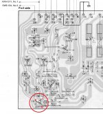
Now I'm so much in doubt exactly how to place the leads on Q3 on the board. I'm sitting trying to make the correct pairing, and right now I believe that :
1. emitter goes into the hole nearest the corner where it says '13V' and 'Q3' on the foil print
2. collector goes into the hole towards the center of the board , and
3. base goes into the hole closest to the long edge of the board just above the '0' in '2SA850'
emitter is the left lead when transistor has flat edge up, leads pointing to me
collector is center and base to the right.
Please advise
Like this:
https://drive.google.com/file/d/0B-K7vfu8iewrT1FNRDJHOGplYUE/edit?usp=sharing
Last edited:
- Status
- Not open for further replies.
- Home
- Amplifiers
- Solid State
- Pioneer SX-1080, after re-cap problem w. center voltage & idle current