#1001 post
I also made 2 pairs output with source resistor (or jumper if not need)...
I'm waiting your new version...
I have my own layout but the parts are not yet complete (on their way)
I'm waiting the parts (vertical mounted 5 watt resistor) so it is fit nicely at the PeeCeeBee
ps : I feel sorry for my earlier post, hope you don't mind
Hi Shaan, I'm 27 🙂I'm grateful to have so many constructive comments that only helps broaden my knowledge and experience. I'm happy to have the chance to share the layout with everyone here, and thankful to the big bros who shared their own works (I'm only 28 🙂 ).
No, you not the only one.Alright, zobel resistor flattened, triangle and line footprint MT trimpot added with single turn trimpot. Seems there will be only one version of the layout. 🙂
I also made 2 pairs output with source resistor (or jumper if not need)...
I'm waiting your new version...
I have my own layout but the parts are not yet complete (on their way)
I'm waiting the parts (vertical mounted 5 watt resistor) so it is fit nicely at the PeeCeeBee
ps : I feel sorry for my earlier post, hope you don't mind
Assuming we are, this is how the mt-POT version's front-side will be.
I think it's best to make two versions, one for cheap single turn and another for multiturn. No space for adding both in one.
Shaan, there is top adjust version with same footprint as side adjust
...hope you don't mind...
Not at all. 🙂
Shaan, there is top adjust version with same footprint as side adjust
How is this one? The all in one! 😎
Attachments
No, you not the only one.
Of course not. But what I meant in that post is that initially I planned to make two layouts, one for single turn pots and another for multiturn, and that now I will post only one. That's it.
I have seen your layout, it's cool.

Of course not. But what I meant in that post is that initially I planned to make two layouts, one for single turn pots and another for multiturn, and that now I will post only one. That's it.
I have seen your layout, it's cool.
It's prefect Shaan!! 🙂🙂🙂
Thanks
...I will try to take a close look tomorrow...
Hi Pete.
Waiting for your input.
The Renesas parts I have measure consistent in thickness, 4.8~4.85 mm.In the meantime, interested guys may start sourcing 1.5mm or 1.6mm thick nylon washers for the VAS. These will be our "spacers". 😉
The BD139/140, not so much, but mostly around 2.5~2.55 mm
(TO-126 w. heatsink pkg)
The BD139-16S-16/140-16S are between 3.25 and 3.30 mm
(those are all-plastic, so different pkg spec)
KSA1381/KSC3503, also plastic, same 3.25 ~~ 3.30
My mica washers measure 0.1 mm, and my silpads, 0.32
just for comparison....
LC used the Alfets, 5.02-5.03 mm with an insulator 0.33 thick
KSA1381/KSC3503 plastic pkg, about 3.25 mm (no insulator required)
and 2 mm spacers
@Shaan, still planning to respond to the layout, been a bit busy, sorry
One can use two spacers if one isn't enough, simple.
Alright, the pdfs will be posted here once Pete gives it a 'go'.
That said, the pdfs for the current layout is ready. So if anyone wants them, just send me a PM with your email address. Easy.
Cheers.
Alright, the pdfs will be posted here once Pete gives it a 'go'.
That said, the pdfs for the current layout is ready. So if anyone wants them, just send me a PM with your email address. Easy.
Cheers.
Shaan,
I think it is a very nice and clean layout, and it places the dual mosfets and VAS transistors very well now.
The 470R which was in paralel w the two diodes is absent, so I assume you are planning on a fixed voltage spread. I would not have a problem with that, but it may be worth noting for other people.
The diameter of the largest electrolytic is 16-mm (?)
That's all from me,
Pete
I think it is a very nice and clean layout, and it places the dual mosfets and VAS transistors very well now.
Sure, I do not see a big issue, but since I have a bunch of parts sitting here, I thought I would post some dimensions, so we can all plan ahead.One can use two spacers if one isn't enough, simple.
The 470R which was in paralel w the two diodes is absent, so I assume you are planning on a fixed voltage spread. I would not have a problem with that, but it may be worth noting for other people.
The diameter of the largest electrolytic is 16-mm (?)
That's all from me,
Pete
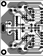
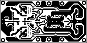
PEECEEBEE V2.0 Double MOSFET
Dimensions: 5" x 2.5" (127mm x 63.5mm)
Have fun.
🙂


...
..
.
Dimensions: 5" x 2.5" (127mm x 63.5mm)
Have fun.
🙂
...
..
.
Attachments
I think it is a very nice and clean layout, and it places the dual mosfets and VAS transistors very well now.
Thanks for your help.
The 470R which was in paralel w the two diodes is absent, so I assume you are planning on a fixed voltage spread.
Pads have been added for trimmer(470R or 1K). So if one wants to play with the bias then replace the 4148 diodes with the trimmer.
The diameter of the largest electrolytic is 16-mm (?)
0.4" (10.2mm) 🙂
Again thanks for the time you spent on scrutinizing the layout. Big help.
Hi Shaan,
Do you have the official BOM for this double MOSFet PeeCeeBee V2 Amplifier?
Btw, given the lengthy threads, how did you implement this for a subwoofer amp?
Thanks again for the nice PCB design.
WP
Do you have the official BOM for this double MOSFet PeeCeeBee V2 Amplifier?
Btw, given the lengthy threads, how did you implement this for a subwoofer amp?
Thanks again for the nice PCB design.
WP
Dimensions: 5" x 2.5" (127mm x 63.5mm)
Have fun.
Now PeeCeeBee has the option to run on higher voltage, say 50V. This is in fact as using double die Latfets but much cheaper as double die Latfets cost 10 Euros each. Also the cooling will be better than single double die Latfet.
No doubt that the builders will have fun!
can someone tell me please how to order pcbs. Thanks Evette
Do it yourself !
🙄
Hi Shaan,
Do you have the official BOM for this double MOSFet PeeCeeBee V2 Amplifier?
Btw, given the lengthy threads, how did you implement this for a subwoofer amp?
Thanks again for the nice PCB design.
WP
My pleasure.
I haven't built the dual FET PCB yet. But I intend to drive it with ESP subwoofer processor.
Now PeeCeeBee has the option to run on higher voltage, say 50V. This is in fact as using double die Latfets but much cheaper as double die Latfets cost 10 Euros each. Also the cooling will be better than single double die Latfet.
Correct.
can someone tell me please how to order pcbs. Thanks Evette
Hi Evette.

You can ask guys in this thread who have built it successfully and are close to your residence, through PM. The dual FET PCB hasn't yet been built by any.
Or, if you are in a hurry, then how about etching it yourself and show it off here, will be great.
shaan
Do you have the official BOM for this double MOSFet PeeCeeBee V2 Amplifier?
Not yet. It's cooking. Please wait.
Important: Non-critical error in Silcscreen of Dual FET PEECEEBEE V2
The 10R and 470R resistors at the positive VAS got swapepd. Apologies. I'm still a fresher in this field. 😱
Please note:- The devices will not fail if someone places them in swapped positions following the faulty silkscreen.
What will happen:- The VAS and Output stage simply will not turn on, there will be no danger for the circuit or speaker(if connected).
The corrected silkscreen is in the next post.
Attachments

- Home
- Amplifiers
- Solid State
- PeeCeeBee