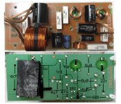
pcb experts, I'm making some test boards to perfect the use of kiCad and I ask you
- the fixing holes on the board, should they be indicated and if so, how?
- and even if you can have a preview of the finished tracks on the back of the card?
- the fixing holes on the board, should they be indicated and if so, how?
- and even if you can have a preview of the finished tracks on the back of the card?
Indicated how? I some time will label them with intended screw size, like M4.
Don't really understand that last question?
Don't really understand that last question?
for the preview I solved it. it was about display settings. while for the holes, where should they be drawn?
ok, 👍
i'm still doing various tests. now i can also have a preview with the components in 3D and you can also see the tracks behind the board.
what do you think about this version?

i'm still doing various tests. now i can also have a preview with the components in 3D and you can also see the tracks behind the board.
what do you think about this version?
Are you going to leave these tracks and clearence to other joints like this? You have got plenty of space and no need
to waste copper.
to waste copper.
Widen your tracks as much as possible. Also, make the pads for the mounting holes as large as practical; the components are physically large, and this will add reliability to the mounting. For the caps, consider putting a pair of holes at 90 degrees to the axis of the cap to feed a tie wrap through. Be careful running tracks under air core inductors—consider the direction of the fields and whether you will be coupling to other components.
I would recommend a terminal strip with screws to connect your offboard wires. It will make it much easier when you have to take it out. Phoenix and Cinch make good ones. Most board manufacturers start the process with a dual-sided board, even if you order a single-sided one. (They etch off one side entirely!) If you have two sides of copper, use them! A simple trick I have used in high-current boards is creating duplicate, parallel tracks on top and bottom, cutting the track resistance in half.
I would recommend a terminal strip with screws to connect your offboard wires. It will make it much easier when you have to take it out. Phoenix and Cinch make good ones. Most board manufacturers start the process with a dual-sided board, even if you order a single-sided one. (They etch off one side entirely!) If you have two sides of copper, use them! A simple trick I have used in high-current boards is creating duplicate, parallel tracks on top and bottom, cutting the track resistance in half.
now the tracks are at 0.3mm but I widen them to 1mm and the connectors are no longer visible.
this is the updated version with the correct dimensions to fit everything. I could optimize the spaces further and maybe insert the L2 between the capacitor and the L1.

this is the updated version with the correct dimensions to fit everything. I could optimize the spaces further and maybe insert the L2 between the capacitor and the L1.
That looks auto-routed with minimal trace widths. For this where traces carry some current, I would go at least 3mm wide, twice that on the return path. and spread traces apart so etch isn't so critical.
I haven't decided yet who will make them. For now I'm practicing on this 2way 12db that I will make myself, without hand-each, then when I will have perfected the use of kiCad, I will decide who to rely on for a more complex crossover.
n. v:

n. v:
let me understand, those who print the Pcb cards start from a completely copper-plated card that is then cut according to the tracks? I thought they proceeded chemically, applying the copper only where necessary. let me understand.
L. v.

L. v.
Last edited:
AFAIK the copper is either milled or etched away where it should not be. Make that tracks a lot wider but not wider than the PCB pads of parts! Use 2 pin 6.3 mm faston PCB mount connectors and 5.08 mm Phoenix MKDSN connector block footprints for the input and output connections so you can use either of those. You can use 4.8 mm faston PCB mount connectors for the tweeters to avoid mistakes. Soldering wires to boards is asking for trouble with thicker cabling and it is less reliable too. Versatility and serviceability without extra cost is nice.
Beginners mistake: the text "REF**" will be visible on your board. Either delete or change to "M3" or "M4". BTW you just have mounting holes which is good but what about plated through reinforced mounting holes (they are in the library) for extra sturdiness?
Beginners mistake: the text "REF**" will be visible on your board. Either delete or change to "M3" or "M4". BTW you just have mounting holes which is good but what about plated through reinforced mounting holes (they are in the library) for extra sturdiness?
Last edited:
I take note of the suggestions, and I'll look for the connectors you mention. I did a test with 1.5mm tracks

- Home
- Loudspeakers
- Multi-Way
- PCB or not PCB, this is a problem


