Hey Gluca,
Donate my balance to "Save the Children". Think the money works better there. If not, return them to so I can donate them.
same here.....
If you are using IXTP01N100D at Q100 and Q200 you can go up to 1000V as the upper FETs (Q100 and Q200) are taking all the voltage drop.
I'd be surprised if the track to track clearance used will support these high voltages.
Even 400V looks iffy. What specification did you follow in terms of voltage creepage distances?
Last edited:
Hey Gluca,
Donate my balance to "Save the Children". Think the money works better there. If not, return them to so I can donate them.
Mine is same. Thanks!
to luvdunhill
input to output voltage diff is typically in the 200V ballpark as a maximum and only a couple points in the PCB (~1mm distance) might experience that difference while difference to GND (connection to GND is optional anyway through the upper-left mounting hole) can be as high as 4-500V typically. all that said, I have other preamp boards I packed as the one of the GB and running at 500V with no issues since ages.
suggestion to use IXTP01N100D is mainly because that FET proved to be much more reliable and sturdy to startup spikes (in my experience) than the DN2540. usual disclaimers while working with tubes and high voltages apply.
to gmant123
I have a spice model running ... I'll try to post a few simulation if I find a few spare minutes
Originally Posted by revintage
Hey Gluca,
Donate my balance to "Save the Children". Think the money works better there. If not, return them to so I can donate them.
Same here. Thanks for the GB.
input to output voltage diff is typically in the 200V ballpark as a maximum
yes, i do not expect to use it at more than that......having a mosfet rated for 1kv gives you some peace of mind.....
to luvdunhill
input to output voltage diff is typically in the 200V ballpark as a maximum and only a couple points in the PCB (~1mm distance) might experience that difference
Wouldn't the input and output pads of the top FET (which I assume are less than 1mm apart) experience this voltage differential?
I think using the ground connection is probably bad idea, the distances are very small there.
Even 1mm clearance, assuming the PCB has a solder resist coating, gives a maximum of AC + DC voltage of 327 V according to specifications I see, and if one is in a relatively humid environment, that number drops further.
Just be careful.
Last edited:
Yes the critical distances are exactly on the LND150s pads and one other is in proximity of a pot. Thanks for the hints.
Hi Gluca,
If you wind up out-of-pocket on anything with the GB please apply my $$ to that first, otherwise donate to DIY Audio. Thanks again for all your time and effort! The board looks great.
If you wind up out-of-pocket on anything with the GB please apply my $$ to that first, otherwise donate to DIY Audio. Thanks again for all your time and effort! The board looks great.
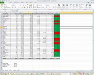
I mailed the very last envelopes this morning. Here it is the balance with all the payment received so far ... I'll wait more days to collect all the remaining money before donating.
A few more hints on the boards.
I usually set before the current of the CCS using a 9V or 12V battery and that is strongly suggested. In case you will be using the VCCS (install Q102* and Q202* and other optional parts, install >0.1uF hi voltage rated caps at the bypass jumpers) you'd better set the CCS current as before and then install Q102* and Q202* and adjust the gate voltage at the lower FETs (Q101 and Q201) which sets the output voltage.
Attachments
How high should the voltage rating be?0.1uF hi voltage rated caps at the bypass jumpers)
At startups the voltage across that cap can be the full B+ so I'd say the classical 630V film would be OK (I am assuming you are working with 'standard' tube voltages in the range of 3-400V and not 1kV).
hey Gianluca, go get yourself a hamburger and coca-cola with fries......my treat.....you have been working hard.....
Ok,I have a pair of 0,47uF/630Volt cam I use them?so I'd say the classical 630V film would be OK
Ok,I have a pair of 0,47uF/630Volt cam I use them?
Yes, they would be OK
- Status
- Not open for further replies.
- Home
- Group Buys
- PCB for cascoded IXYS CCS (tube)