hello,
can someone please help me here,
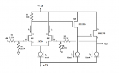
i do not completely understand how much current needed for input and output fet
when using K170 as input, and ZVN/ZVP mosfet as output
the current source needed are:
i1 = 4mA
i4 = 10mA
i6 = 10mA
if i am using J309 for input, BS250 vas, BS170 output.
what about the i1 i4 i6 as ccs? is it still the same with K170 jfets?
voltage rails are 15vdc
thanks.
can someone please help me here,
i do not completely understand how much current needed for input and output fet
when using K170 as input, and ZVN/ZVP mosfet as output
the current source needed are:
i1 = 4mA
i4 = 10mA
i6 = 10mA
if i am using J309 for input, BS250 vas, BS170 output.
what about the i1 i4 i6 as ccs? is it still the same with K170 jfets?
voltage rails are 15vdc
thanks.
Attachments
with J309 in LTP , you can try I1 between 4 and , say, 16mA
more , the merrier
for I4 and I6 , leave them as is
more , the merrier
for I4 and I6 , leave them as is
with J309 in LTP , you can try I1 between 4 and , say, 16mA
more , the merrier
for I4 and I6 , leave them as is
i still don't understand how to determine the current need for each type of jfets
is it from their datasheet, where to look? 🙄
btw is it (current through I1) have to be matched between each channel?
i mean, if left channel set for 6mA then right channel also 6mA?
and about the gain resistors, articles said Rc/Ra (22k1/2k21=10dB)
can i substitute those resistor let say Rc:100R and Ra:10R which result the same in calculation.
thanks.

Last edited:
LTP JFets Iq - it really depends of purpose , making compromise between oomphs and noise and few other things
however , most ppl around agree that 90% of their Idss (datasheet!) is sweet spot , but always taking care of their dissipation
J309 is nothing else than somewhat sorted lower Idss range of J310 ; and even that one is having highish Idss (12 to 25mA , from top of my head)
so , 90% of Idss is pretty much no-no area, when you take sane dissipation in account (that being mA x voltage across device)
result - think of it same as using Toshiba 2SK170BL ....... and they probably will last long in circuit
you need to have matched parts in LTP , but matching between channels is not overly important - as long there is some feedback to equalize things and as long you'r using parts in , say, 25% window
setting is different thing - if you choose ,say, 6mA per device in LTP (or any other stage) , choice is made for both channels ......
gain resistors - that depends ......... gain will always be ratio between said position resistors , but exact value of these is determined by some other things ; without looking at article (so , no checking nomenclature) , say that resistors at input gate are defining input impedance of (discrete) OP ; what you are going to set there is matter of choice , hopefully reasonable one
it could be helpful if you say what you're trying to make , so replies could be more specific ......
and - take care about fact that value of drain resistor is related to current through that LTP Jfet , where voltage across it is related to UGs of following mosfet ......
things are simple , after some mileage even simpler than Papa described them in article
but prior to that (mileage) , they're much more complicated than Papa described them in article
so - advice - install LTSpice and try to learn things ; when you feel cool enough , translate some of your sims in physical realm
after several millions of clicks and few bags of poof devices , you'll know much more
Last edited:
i am building a balanced low pass filter for akm dac,
and i want to replace the opamp with discrete devices.
the opamp to be replace is NJE5534 or LME49710.
do we need to adjust the discrete opamp gain according to previous opamp used?
for balanced, i need four single discrete opamp.
that's mean i need four matched pairs of J309 for input stage,
and i have J309 in hand which have Idss:
pair A : 13.62 and 13.60 (sweet spot 90% of Idss, around 12mA)
pair B : 13.71 and 13.72 (sweet spot 90% of Idss, around 12mA)
pair C : 14.87 and 14.84 (sweet spot 90% of Idss, around 13mA)
pair D : 11.82 and 11.84 (sweet spot 90% of Idss, around 11mA)
is that how we calculate for real current need?
btw many thanks for the explanations, will take times to digest them.
Attachments
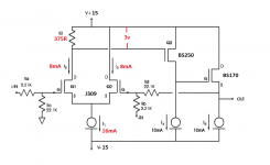
first concentrate on OP developing , gain (resistor values and ratio ) is secondary issue
set LTP current to 8mA per side , for all OPamps you need ;
now - taking Papa's examples , what value of drain resistor you need there ?
set LTP current to 8mA per side , for all OPamps you need ;
now - taking Papa's examples , what value of drain resistor you need there ?
first concentrate on OP developing , gain (resistor values and ratio ) is secondary issue
set LTP current to 8mA per side , for all OPamps you need ;
now - taking Papa's examples , what value of drain resistor you need there ?
8mA per side, did you mean 8mA for one J309? (16mA for one pair)
R2 = 3v/0.008A = 375 ohm
is it correct?
yup , for both
of course , you'll need those surrounding resistors , in time of testing
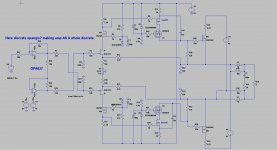
ok 8mA per side, so i will set I1 for 16mA
(i attach the schematic, to make sure)
maybe i will use trimpot to help finding real live value of R2
Attachments
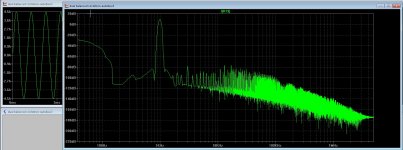
finished solder all components into my prototype pcb's,
except those input resistors (2k2 and 22k)
what i have in hand are 15k and 150k
can i use them to replace 2k2 and 22k??
thanks.
except those input resistors (2k2 and 22k)
what i have in hand are 15k and 150k
can i use them to replace 2k2 and 22k??
thanks.
Attachments

Last edited:
wengtech,
congrats for your attempt
I follow with Interest your progres and would be Interested at final product of pcbs If you are going to order
congrats for your attempt
I follow with Interest your progres and would be Interested at final product of pcbs If you are going to order
finished solder all components into my prototype pcb's,
except those input resistors (2k2 and 22k)
what i have in hand are 15k and 150k
can i use them to replace 2k2 and 22k??
thanks.
2k2 is gate stopper (anti-oscillation thingie)
22K is in same time establishing two things - gate potential (gnd) and input impedance
in place of 2K2 use anthing between 330R and 3K3
for 22K position use whatever you have in range of 15K to 100K
remember - for proper operation of OP , you also need to connect two feedback resistors

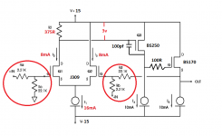
in your case , you need entire shebang , with appropriate values
so , referring to left schematic : R2,R1,C3,R3,C2 ( all in pos. input side network) , and R4,R5 (both in negative input side network)
so , referring to left schematic : R2,R1,C3,R3,C2 ( all in pos. input side network) , and R4,R5 (both in negative input side network)
in your case , you need entire shebang , with appropriate values
so , referring to left schematic : R2,R1,C3,R3,C2 ( all in pos. input side network) , and R4,R5 (both in negative input side network)
do you mean i can ignore those Ra,Rb,Rc,Rd network in the discrete opamp
and connect directly to resistors network at the LPF board, correct?
now is a moment when you really need some reading , and only then proceeding with puzzle approach
any OP amp dedicated book will be good
try this one (I uploaded it for occasions like this one ) :
https://dl.dropboxusercontent.com/u/20665608/For DiyAudio.rs/ELECTRONICS_A_Complete_Course.rar
see chapter 15
any OP amp dedicated book will be good
try this one (I uploaded it for occasions like this one ) :
https://dl.dropboxusercontent.com/u/20665608/For DiyAudio.rs/ELECTRONICS_A_Complete_Course.rar
see chapter 15
now is a moment when you really need some reading , and only then proceeding with puzzle approach
any OP amp dedicated book will be good
try this one (I uploaded it for occasions like this one ) :
https://dl.dropboxusercontent.com/u/20665608/For DiyAudio.rs/ELECTRONICS_A_Complete_Course.rar
see chapter 15
wow... that was a very-very complete course 😀
thank you very much ZM
Hi All
Did see this interesting thread, I have a allfet circlotron thread and want to use opamps as unbalanced to balanced input, because it is a allfet, It is fun to use also allfet opamp and you guys are busy with that, so may I use this discrete into the allfet>?
thanks.
Did see this interesting thread, I have a allfet circlotron thread and want to use opamps as unbalanced to balanced input, because it is a allfet, It is fun to use also allfet opamp and you guys are busy with that, so may I use this discrete into the allfet>?
thanks.
Attachments
Last edited:
- Status
- Not open for further replies.
- Home
- Amplifiers
- Pass Labs
- Pass Discrete Opamp in DIP-8 Package