Re: Re: Re: Re: check this out .....
probably nico was refering to my previous post regarding not matched ltp pair and also with no thermal junction .....
a non matched ltp pair will probably have diferent offset behaviour and of course this will be also temperature depending since there is no thermal junction
AndrewT said:why would two matched BJTs have different dT/dt? I thought this was pretty near fixed by the physics.
Different Dt/dt is not what shows when a matched pair are in the jig.
However, when testing jFETs, then they definitely have different slopes, and one has to find similar Idss and similar slopes, to then select matched pairs. The slope is effectively Gm.
probably nico was refering to my previous post regarding not matched ltp pair and also with no thermal junction .....
a non matched ltp pair will probably have diferent offset behaviour and of course this will be also temperature depending since there is no thermal junction
Re: Re: Re: check this out .....
hello all to you.
hello dear nico ras.
didn't you think of:......,and better of glued together?
greetings...........
Nico Ras said:
then they will perform differently, and worse if glued together.
hello all to you.
hello dear nico ras.
didn't you think of:......,and better of glued together?
greetings...........
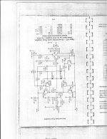
layout .....
looks very nice and symmetric ( the type of pcb i would like to built )
i will ring a bell though .... here are some thoughts of forum member EVA that took a second and bother with the same issue in another thread .....
******0.1mfd decoupling have no serious effect if located like that IE next to ground taking also in mind that both rails traces are quiet long .... they are too far away fro outs ( evas opinion about this is that it only works good if located next to ground and very next to outputs )
****** then this long trace of out put can aslo cause complications ..... out resistors should be as close possible
****then again signal ground eventhough equiped with 10 R resistor to create a more "clean" ground is quiet long
****** and finally ltp has no option for thermal junction ( that could be very nice also ....
ONE THING i clearly dont like is the resitor tha feeds the ltp second transistor from out put ....this to me looks like a very nice capacitor ...this is something i would never do
eva's ideal pcb was something that had power caps almost in the midle ( we talked about that also ) power caps included on board very possible since this amp will work with 2*10.000 mfd on board ...so caps are on the midle with all power ,out and ground conectors next to them .... just behind the caps the power trs and on the totally other side the small stuf like ltp vas and other stages .....
the goal of all this is to achive the most minimum distortion .....
after studing this for very long ....if you need to fullfill all these specs then this cannot be done in single side pcb ....
and this arize the question if an amp like that worth such an effort IE double side pcb /extreme design....
other wise pcb looks just fine
best regrads sakis ( with very sexy avatar )
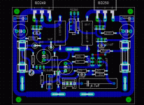
 Now build it.
perfect enough ....
this is more or less they lay out i ve done ...with a few minor changes .....
this will work with out any problems at all ....( eva's idea about decoupling and so cannot be done here but we talked about that in a previous post )
only one thing .....
bc transistor that is located top midle is the VBE multiplier CANNOT !!!be attached to the heat sink ( please read carefully rod's recomenation about all that )
though it can be stilllocated there but not attached to the heatsink
nice rounded corners well done !!!!!
I build P3A amp, work good and is cheap, I used Q4, Q5, Q6 BD139,140 and output MJE2955/3055 (60W/ 8 ohms)
Some observations:
-Q5 and Q6 Not in heatsink TR's output , Nor need heatsink they operate in class B
-Q4 Need heatsink in +-42V
-Q9 Not is heatsink (according to Elliott),I not put Q9 to heatsink, noticed some instability not colled after work. More low temperature to turn without signal (music),is a little more force signal not back to state low temperature, does not affect more and works well for hours
This design P3A has many limitations, The first stage is too loaded (gm) to compensate for low Beta the second stage, if improved will be Blameless.
Best build directly Blamelles of book 😀
Some observations:
-Q5 and Q6 Not in heatsink TR's output , Nor need heatsink they operate in class B
-Q4 Need heatsink in +-42V
-Q9 Not is heatsink (according to Elliott),I not put Q9 to heatsink, noticed some instability not colled after work. More low temperature to turn without signal (music),is a little more force signal not back to state low temperature, does not affect more and works well for hours
Havenwood said:Originalmente postado por Havenwood [/ i]
[Whit Re1 = RE2 = 100ohms.
E adicionar Re (Q1) = Re (Q2) = 22ohms? (constante degeneração gm)
Olha Audio Power DesignHnadbook por Dougles Self pag84.
Gostaria de saber a sua opinião
This design P3A has many limitations, The first stage is too loaded (gm) to compensate for low Beta the second stage, if improved will be Blameless.
Best build directly Blamelles of book 😀
you are right......you layout was my sourse of inspiration......the transistor that you are talking about I will replace it with a BD139
Which Tr's (Q9 )?Adi_007 said:the transistor that you are talking about I will replace it with a BD139
p3a improvement
Hi, I think that this amp can be improved by changing output trans to darlingtons and increasing the driver load resistors to say 2k and adding two resistors from driver emitter to ouput collector. thus the output stage becomes a 'triple'. Mr jl hood has used this. I would appreciate feedback P!😀
Hi, I think that this amp can be improved by changing output trans to darlingtons and increasing the driver load resistors to say 2k and adding two resistors from driver emitter to ouput collector. thus the output stage becomes a 'triple'. Mr jl hood has used this. I would appreciate feedback P!😀
I don't like the inflexibility of integrated darlingtons. They have been invented to make PCB assembly cheaper. Not to increase performance of an amplifier.
If the output stage does not have sufficient current gain, then add a pre-driver to create the triple T output stage and thus get the current gain you need.
If the output stage does not have sufficient current gain, then add a pre-driver to create the triple T output stage and thus get the current gain you need.
Re: p3a improvement
andrew is right .... you can not expect anything from darligtons ..... ( best example NO comercial amp is made with them )
p robertson said:Hi, I think that this amp can be improved by changing output trans to darlingtons and increasing the driver load resistors to say 2k and adding two resistors from driver emitter to ouput collector. thus the output stage becomes a 'triple'. Mr jl hood has used this. I would appreciate feedback P!😀
AndrewT said:I don't like the inflexibility of integrated darlingtons. They have been invented to make PCB assembly cheaper. Not to increase performance of an amplifier.
If the output stage does not have sufficient current gain, then add a pre-driver to create the triple T output stage and thus get the current gain you need.
andrew is right .... you can not expect anything from darligtons ..... ( best example NO comercial amp is made with them )
I will use for output 2SC5200/2SA1943, driver transistors MJE340/350 and for input BF422.... are these transistors good?
darlingtons on p3a
I am sure that i'm correct as the triple so formed will have a very input impedance thus the VAS works with very light loading.The late jl-hood can't be wrong. see hifi news&record review 1980.
anyway its a simple way of improving performance without too many modifications!
I am sure that i'm correct as the triple so formed will have a very input impedance thus the VAS works with very light loading.The late jl-hood can't be wrong. see hifi news&record review 1980.
anyway its a simple way of improving performance without too many modifications!
It would be better to use BD139/140 or MJE243/253 for drivers than MJE340/350 which do not handle much current. You can use MJE350 for VAS.
The BF422's are high voltage but low fT, 2N5550/1 are better here and easy to get. 80Vceo is enough, and look for something with a low NF and fast fT.
Make sure your 2SA1943/2SC5200 devices are genuine. If you bought them very cheap, they are fakes, especially if they are branded as Toshiba.
The BF422's are high voltage but low fT, 2N5550/1 are better here and easy to get. 80Vceo is enough, and look for something with a low NF and fast fT.
Make sure your 2SA1943/2SC5200 devices are genuine. If you bought them very cheap, they are fakes, especially if they are branded as Toshiba.
One way to improve design P3A is replaced the bootstrap(formed by R9, R10 and C5)a source of current and then degenerate input pair
Yes can use TR's in output another good option would MJ802/MJ4502, The TR's BF422 I do not know, if beta equal that Bc, can use no problem...Adi_007 said:I will use for output 2SC5200/2SA1943, driver transistors MJE340/350 and for input BF422.... are these transistors good?
Re: darlingtons on p3a
Triples are good, but to be honest the P3A is a simple circuit. If you want to go the way of triples, there are many other things to correct with the P3A circuit first. Personally, i think the Sziklai pair output stage is more hassle than its worth.
p robertson said:I am sure that i'm correct as the triple so formed will have a very input impedance thus the VAS works with very light loading.The late jl-hood can't be wrong. see hifi news&record review 1980.
anyway its a simple way of improving performance without too many modifications!
Triples are good, but to be honest the P3A is a simple circuit. If you want to go the way of triples, there are many other things to correct with the P3A circuit first. Personally, i think the Sziklai pair output stage is more hassle than its worth.
- Home
- Amplifiers
- Solid State
- P3A layout