yes, the right and left side parts are identical.
No, they are not. Take a look at the file attached.
Attachments
because the FETs heating without the loads already
No wonder: high-side transistor has nowhere to pour out it's gate charge before low-side transistor opens, and this is the shoot-through reason.
So...
I don't really understand why to measure (only) without load.
+1 Thats right!
Harder gate pull down, or increased Cgs may help!
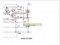
And I would add: You've got BAD input front(s) - as I mentioned in my previous post - make them GOOD.
Last edited:
by saying "identical" I mean on the basis of components.No, they are not. Take a look at the file attached.
you're right, the input signals are not symmetrical. but we are talking about 1-2nS of difference!
if we think the dead time is about 45nS, it is a small difference and no problem i think!
I tried to make match the outputs (it is TL3016's inverted outputs) but whatever I done is not work and then I pushed to the background to solve after shoot through problem.
you're right, the input signals are not symmetrical. but we are talking about 1-2nS of difference!
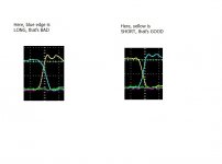
It is not plain difference that matters, but LONG (bad) rear-edge as itself.
Make it SHORT (good).
correct me if I'm wrong but gate charge of the high side FET can pour out through the fet driver IC it has source and SINK! capability. I dont think this is a shoot through reason. can you explain im more detail..?No wonder: high-side transistor has nowhere to pour out it's gate charge before low-side transistor opens, and this is the shoot-through reason.
And I would add: You've got BAD input front(s) - as I mentioned in my previous post - make them GOOD.
is that really matters 1nS of deviation?
but LONG (bad) rear-edge as itself.
Make it SHORT (good).
forgive me to make you explain everything twice. but I couldn't understand wht do u mean by "LONG","SHORT"..?
correct me if I'm wrong but gate charge of the high side FET can pour out through the fet driver IC it has source and SINK! capability. I dont think this is a shoot through reason. can you explain im more detail..?
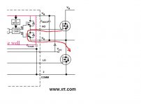
Off course. Look at the attachment.
Red line is the sink (or pour-out) way. So, without load, gate charge goes through lower-side transistor.
In Your case, without load, charge has no way to go unless lower-side transistor is opened.
Later, when lower transistor gets opened, higher one is still opened either. What is the concequence? Right, shoothrough.
Attachments
Last edited:
forgive me to make you explain everything twice. but I couldn't understand wht do u mean by "LONG","SHORT"..?
Yes, shure.
Attachments
is that really matters 1nS of deviation?
Unfortunately... But not the deviation, a BAD edge as itself can result in undefuned states in logics followed by driver output's "faultstarts".
Last edited:
Off course. Look at the attachment.
Red line is the sink (or pour-out) way. So, without load, gate charge goes through lower-side transistor.
In Your case, without load, charge has no way to go unless lower-side transistor is opened.
Later, when lower transistor gets opened, higher one is still opened either. What is the concequence? Right, shoothrough.
the reference of the bootstrap circuit is not ground. So why the current chose the way to gnd? the discharge path according to my knowledge:
Attachments
Yes, shure.
yes that could be a reason for the driver IC to be unstable.. I knw it must be repaired but I did not think it as a big problem. I'll work on it.
PNP pull down, or UCC27200 gate driver (for example).
you mean low impedance gate drive i think AN-937 by IRF 🙂
this is reasonable..
1050/50=21
yes with a rough calculation it must be: but I take the measurements and it nearly "x25" may be loading effect again?
Maybe You can recommend TO-220 FET for this application?
Thank You in advance.
For below 60V IRFB3806 are the best.
For 60 to 75V you can try more powerful IRFB3607.
Very critical timing between two independent half bridges?
Impossible to discharge a capacitor by shorting their legs?
Choosing devices with higher switching loss when switching loss is already dominating?
I think I'm too old.
Impossible to discharge a capacitor by shorting their legs?
Choosing devices with higher switching loss when switching loss is already dominating?
I think I'm too old.
14nC Qgs, 5nC Qgd mosfets, 100kHz, low inductance (wide soft switching area), pardon me, what switching losses?
Too high ripple current, false miller triggering, too high di/dt and shoot-through are possible problems for overheating and choosing IRFB3806 with slightly higher charges, lower Rdson, faster body diode and some helpful internal inductances is IMHO going to make things a bit better.
Too high ripple current, false miller triggering, too high di/dt and shoot-through are possible problems for overheating and choosing IRFB3806 with slightly higher charges, lower Rdson, faster body diode and some helpful internal inductances is IMHO going to make things a bit better.
Since this is effectively two bridged single-ended amps, it occurs to me that testing each independently might throw some light on the problem. At least it would tell you if it's a component/wiring fault on one side, or a design fault that affects both. Basically you'd just need a DC-blocking capacitor to ground in place of the output stage not being tested. In fact it probably wouldn't need any board mods to try that, just add an external hardwired HF filter, load and cap.
At least you'd then be armed with the knowledge that either both sides behave identically, or that one side shows an anomaly.
If this has already been tried, apologies as it's a long thread.
At least you'd then be armed with the knowledge that either both sides behave identically, or that one side shows an anomaly.
If this has already been tried, apologies as it's a long thread.
14nC Qgs, 5nC Qgd mosfets, 100kHz, low inductance (wide soft switching area), pardon me, what switching losses?
The one that heats them up over 100 Celsius . Fsw is not 100 kHz, but 800 originally.
Too high ripple current,
This was my first idea also, and this because I asked fsw and inductance. But it was not the reason.
false miller triggering, too high di/dt and shoot-through are possible problems for overheating and choosing IRFB3806 with slightly higher charges, lower Rdson, faster body diode and some helpful internal inductances is IMHO going to make things a bit better.
Body diode is really faster, thanks to the lower voltage rating, but there are faster DirectFETs also. And tr=40 ns and tf=47 are very much! (Compared to 5 ns of IRF6645.)
However maybe I judged too fast, because it was specified at Rg=20. With lower Rg it will surely better, but can't tell how much.
Anyway: changing the whole circuit before knowing what is the real problem, doesn't seem to be wise.
Last edited:
For below 60V IRFB3806 are the best.
For 60 to 75V you can try more powerful IRFB3607.
Thanks, darkfenriz!
Last edited:
Too high ripple current, false miller triggering, too high di/dt and shoot-through are possible problems for overheating
Apologies for lil' offtopic.
What is "ripple current" as far as output FET concerned?
Small deviations of current running through it, when FET channel is opened?
Would be kind of You to explain.
Last edited:
- Status
- Not open for further replies.
- Home
- Amplifiers
- Class D
- Output transistor temperature changes with load characteristics..