yes - it is better to keep things simple - but not to simple 😀 simple enough to sound really really good 😀 or something like that 😀
do You think it would benefit from those ccs's... and where to put them ... on predriver or on driver transistors ... i think better on driver transistor ..... regards
daniel
do You think it would benefit from those ccs's... and where to put them ... on predriver or on driver transistors ... i think better on driver transistor ..... regards
daniel
In my mind: two emitter coupled Alephs in compliment, as
one giant voltage following diamond buffer... But Pass said
it looked to him more like Hawksford or Cordell...
At that time, both my input buffering and error comparing
transistors were bipolar. Which was stable reference for
comparing and correcting an error, but not great in other
ways (like bandwidth).
So now we have JFETs as source coupled gate followers?
Theory of operation hasn't really changed all that much....
Only the components chosen somewhat better. You might
have to tweak the little resistors in the middle to balance
the diamond. Use of matched pair JFETs 2SK389/2SJ109
would probably help.
Don't know if its good enough to qualify for your purpose,
but I was thinking to follow up after an Aikido...
Its biased into Class AB with a real smooth crossing. If you
bias with intention only for Class A, then Schottky nonlinear
resistances in the output can be omitted.
C1 seems necessary to quench oscillation? It may just be
LTSpice, but maybe it stores energy equal to the MOSFET
gates? I'm not really sure why it sims so much better with....
Attachments

Yes, probably similar. Hard to tell without working values to plug
into the sim. Where exactly does yours smooth the AB crossing?
into the sim. Where exactly does yours smooth the AB crossing?
kenpeter said:Yes, probably similar. Hard to tell without working values to plug
into the sim. Where exactly does yours smooth the AB crossing?
When diodes start conducting to the ground. Actually, when one opamp goes to class B due to increased (through diode) current in LTP tail, the complementary opamp stays in class A region.
Values depend on transistors. Values in current mirrors depend on Rbb of output transistors and selected ratios. Values of "short" tails are selected to deliver peak output current divided by a mirror ratio. Values in "long" tails again depend on mirrors' ratio, but supply enough current until long tails start supplying the current.
In reality, I had 4 trimmers in tails. But for IC trimming would not be needed: geometry works instead.
Wavebourn said:
When diodes start conducting to the ground. Actually, when one opamp goes to class B due to increased (through diode) current in LTP tail, the complementary opamp stays in class A region.
Values depend on transistors. Values in current mirrors depend on Rbb of output transistors and selected ratios. Values of "short" tails are selected to deliver peak output current divided by a mirror ratio. Values in "long" tails again depend on mirrors' ratio, but supply enough current until long tails start supplying the current.
In reality, I had 4 trimmers in tails. But for IC trimming would not be needed: geometry works instead.
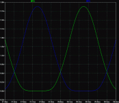
Class B working fine, but no luck finding a bias point for AB.
What am I doing wrong?
Silicon diodes not shuting down quiet as I'd like either...
If its not merely the symptom of my improper bias, I think
a series pair of Schottkys with similar voltage drop might
be smoother...
I throw in the models that I used for output transistors.
I've hacked my default library, if your LTSpice can't find
the needed model, I may have pointed the wrong place.
Attachments
kenpeter said:
Class B working fine, but no luck finding a bias point for AB.
What am I doing wrong?
Decrease long tail resistors (to rails, with no diodes in series).
Also, try Shottkys in class B tails (with diodes to ground), so less class A bias current will be needed. Increase mirrors' ratios for higher OL gain.
kenpeter said:OK, after playin with it a while I kinda got AB to smooth out...
Are these resistor values closer to right?
Looks right. Try load on twice lower resistance and see what happens. It should turn into a current output stage instead of voltage output one.
And I forgot to attach JFET models you need for my first circuit.
.model J2sk170 NJF(Beta=59.86m Rs=4.151 Rd=4.151
+ Betatce=-.5 Lambda=1.923m Vto=-.5024 Vtotc=-2.5m
+ Cgd=20p M=.3805 Pb=.4746 Fc=.5 Cgs=25.48p
+ Isr=84.77p Nr=2 Is=8.477p N=1 Xti=3 Alpha=10u
+ Vk=100 Kf=111.3E-18 Af=1)
.model J2sj74 PJF(Beta=92.12m Rs=7.748 Rd=7.748
+ Betatce=-.5 Lambda=4.464m Vto=-.5428 Vtotc=-2.5m
+ Cgd=85.67p M=.3246 Pb=.3905 Fc=.5 Cgs=78.27p
+ Isr=129.8p Nr=2 Is=12.98p N=1 Xti=3 Alpha=10u
+ Vk=100 Kf=26.64E-18 Af=1)
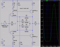
kenpeter said:And here's what my circuit makes of the same signal....
Blame the smoothness on Schottky...
Yes, your amp turns into class B smoother.
Mine was designed as a bullet-proof guitar tube amp output: it protects itself against overload (shorted output or wrong cab connected) refusing to provide more current: it turns into a current output amp when overloaded.
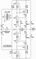
Two stage MOSFET input buffer. It has quite high input impedance, even more than 100kohms.
Sajti
An externally hosted image should be here but it was not working when we last tested it.
Sajti
The 3 deep darlington version, vith current regulator diodes.
Sajti
An externally hosted image should be here but it was not working when we last tested it.
Sajti
sajti said:Two stage MOSFET input buffer. It has quite high input impedance, even more than 100kohms.
An externally hosted image should be here but it was not working when we last tested it.
Sajti
At DC maybe... Those gates won't charge/discharge themselves.
Without a change in gate charge (repeated every cycle) there is
no change in channel current. Regardless how much "capacitance"
a source follower topology might claim to hide, the energy wasted
over time goes up with frequency...
I've actually had to bump up the quiescent current in my drivers
25mA just to swing 100uA into and out of the gates fast enough.
I know that don't sound like good math, but I assure you...
- Status
- Not open for further replies.
- Home
- Amplifiers
- Solid State
- output buffer for a hybrid amplifier