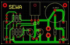
Thanks Mad for the help and for your PCB plan!
I posted a wrong (not ready) PCB plan, but now here is the good one.
I hope it is O.K. 😉
Yes, I like yours much more!😀
Greets:
Tyimo
There is an error in the gate bias circuit.
I posted a wrong (not ready) PCB plan, but now here is the good one.
I hope it is O.K. 😉
I would have designed it much denser though I recommend to have holes for standoffs/pcb mounting in the front corners also.
Yes, I like yours much more!😀
Greets:
Tyimo
Attachments
new schematic questions
One more question:
Why did you changed the value of "so many" parts in your 2nd schematic?? Is it better now?
for example:
R4 from 47K to 100K
R6 from 12K to 33K
R5 from 47K to 100K
R1 from 47K to 1M
etc.
I would like to build the original 7W version or even a more powerfull 10W version, but now I don't now which of your schematic is better?
Greets:
Tyimo
For what you want (more power), the first (SEWArA) is the best. This OTAr0pcb shematic was just what I used to compare SEWAr1 and OTAr0 as they where very similar at that particalur point in time. Also, it incorporates all of the things discussed in this thread. Don't worry about it. Most of the values and impedances in the design are arbitrary, and really doesn't matter with regards to the sound. It has more to do with component size/placement and PCB design.
The nice thing about OTA is that it is so simple, it does not really require a pcb. I can draw a 7W schematic for you for hardwiring, if you want 😉
The nice thing about OTA is that it is so simple, it does not really require a pcb. I can draw a 7W schematic for you for hardwiring, if you want 😉
Thanks a lot Mads!!!
It is very kind from you!😉
That last schematic the OTA7r0 is very cool!
Thanks and greets:
Tyimo
It is very kind from you!😉
That last schematic the OTA7r0 is very cool!
Thanks and greets:
Tyimo
Choke loaded OTA questions
Hi! I am here again!😀
After that we was speaking a lot about how to design a choke loaded Source follower amp on the SEWA thread, I moved this theme here. The SEWA is the CCS version and the OTA is the power resistor (and CHOKE) loaded version.
Before I would build the amp I have 2 questions:
-What parts values need to modificate for an amp with:
24VDC, 120mH-3A choke instead of the power resistor? Should I use the original OTA3.5 values?
-How can I calculate the outpower for this amp? I need a correct formula.
Thanks and greets:
Tyimo
I'm not familiar with choke loaded designs, maybe someone a little more enlightened can answer? Nelson? 😉
Hi Mads!
Me too! 😀
Fuling wrote an output power calculation for me:
"If you ignore stuff like saturation voltage and losses in the choke, just divide your rail voltage by 1,414, square the result and divide by the load impedance"
I think it is enough good.
But my first question is still the same:
-What parts values need to modificate for an amp with:
24VDC, 120mH-3A choke instead of the power resistor? Should I use the original OTA3.5 values?
-How can I adjust the bias in the OTA?
Greets:
Tyimo
I'm not familiar with choke loaded designs...
Me too! 😀
Fuling wrote an output power calculation for me:
"If you ignore stuff like saturation voltage and losses in the choke, just divide your rail voltage by 1,414, square the result and divide by the load impedance"
I think it is enough good.
But my first question is still the same:
-What parts values need to modificate for an amp with:
24VDC, 120mH-3A choke instead of the power resistor? Should I use the original OTA3.5 values?
-How can I adjust the bias in the OTA?
Greets:
Tyimo
Bias in the OTA is given by the voltage at the source of the mosfet divided by the load resistance.
Thanks Mads!
How can I calculate the voltage at the source of the mosfet with different supply voltage?
I mean for example on +12V, and +24V?
Tyimo
How can I calculate the voltage at the source of the mosfet with different supply voltage?
I mean for example on +12V, and +24V?
Tyimo
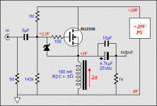
Bias in the OTA is given by the voltage at the source of the mosfet divided by the load resistance.
On the previously attached schematic I see the chokes RDC=0.5R and the voltage at the source is 1V. So, it has really 2A bias!
Until now I was calculating with the choke's RAC. Sorry!
Slowly I will understand the mentality of the choke loaded amps!😀
Greets:
Tyimo
Hi!
I have to recompose my previous question:
I know the Ohm's Law: V=I*R that would give me the source voltage, but what would be the best supply voltage for (with) 1-2 V on the source?
(if my EI core choke would have RDC 0,5-1R and I would like to use 2A bias)
Tyimo
I have to recompose my previous question:
How can I calculate the voltage at the source of the mosfet with different supply voltage?
I mean for example on +12V, and +24V?
I know the Ohm's Law: V=I*R that would give me the source voltage, but what would be the best supply voltage for (with) 1-2 V on the source?
(if my EI core choke would have RDC 0,5-1R and I would like to use 2A bias)
Tyimo
Tyimo said:Thanks Mads!
How can I calculate the voltage at the source of the mosfet with different supply voltage?
I mean for example on +12V, and +24V?
Tyimo
Voltage at the Source= voltage at the gate -VGS of the mosfet (usually 4-4,5V)
Voltage at the gate (latest OTA sch) is= 100K/(100K+27K)*V+ (voltage divider)
Vgate with 24V= 100/127*24=0,7874*24=18,9V
Vsource=18,9-4=14,9V.
Input impedance is essentially the resistor from the voltage divider to the gate (100K).
It would be wise to install a trimpot in the voltagedivider for your choke loaded design since the bias voltage is so low. Like in the BOZ. Alternatively you can paralell resistors acoss the 27K/100K to slightly change their value to get the correct Source voltage.
- Status
- Not open for further replies.
- Home
- Amplifiers
- Pass Labs
- OTA - One Transistor Amplifier