That looks like a cool chip! With one we have I2S and MCLK. In addition a few GPIO lines are needed, but they should be able to go over cheaper and slower isolators.
The GPIO lines I think of are:
- Filter select
- VBUS_EN
- MCLK_P48_N441
- UART TX & RX (it's nice to have some comms link)
- Maybe an interrupt line
Any more lines needed? I imagine making a go-between board between the USB-I2S module and the analog board where the bare minimum of IO lines are isolated and power is inserted.
Børge
Add I2C to your list.
The jitter on the isolator is an issue (100 pS) so its not really suitable as a clock source for the DAC but may be OK if the clocks are on the DAC side. I would latch the data after the isolator on the DAC side just to make it as clean as possible.
1. For the MCLK, the clock source is on the DAC side and only the divided (and maybe latched) clock is passed through the isolator to the uC side. So the 100ps jitter is not an issue.
2. For I2C, you need a bi-directional isolator, such as the ADuM1250, which we have had good results with in another project.
Alex
2. For I2C, you need a bi-directional isolator, such as the ADuM1250, which we have had good results with in another project.
Alex
I2S clocks on the AB 1.1
Hi everybody,
I'm trying to understand better the structure of the I2S interfacing on the AB 1.1, and the inner workings of I2S as implemented on the UC3A3.
Reading the Atmel docs, looking at the code, and seeing the schematics of AB 1.1 I think I ve understood that:
- I2S on the UC3A3 has the limitation that the main clock of the CPU must be synchronous with the clock that drives the SSC module that implements I2C (at least this is what I can understand from the phrase: "Because the master clock must be synchronous to the sample rate both clock sources to the generic clock and to the SSC module must have the same source"
- on the AB 1.1 there are 2 clocks (24.576 and 22.5792 Mhz, the Golledge clocks), one of the two is selected (as a function of the desired sampling frequency, the biggest for 48K and multiples and the other for 44.1K and multiples)
- the selected clock is sent DIRECTLY to the DAC chip, and a divided by 2 version is sent to the CPU (or better, to the power manager, that incorporates PLLs and dividers to create an internal clock to be used by the I2S logic and the CPU).
Now, if I'm not mistaken, the I2S clock is OUTPUT by the UC3 but is unused (the DAC chip is fed directly by the selected clock), while the other signals, mainly LRCLK are generated by the I2S module with internal dividers and counters.
My doubt is as follows:
aren't there any jitter problems on such signals?
The main clock to the DAC comes directly from the high precision Golledge clocks, and that's OK, but LRCLK and SDATA come from the UC3, and so are potentially contamined by internal digital noise ... the UC3 has lots of digital circuitry, with many many different clocks ...
My question (to the experts) is as follows: is it possible on the UC3 to drive the I2S clock from the external? Is the sync between the "generic clock" and the clock of I2S really mandatory?
Moreover, what's the speed of the CPU in this situation? Does it change with selected clock speed? I see in the code that, depending from the desired sampling frequency, the "generic clock" is something between about 3 and 12 Mhz ... is this the speed at which the chip runs while playing?
Last edited:
For the internal of the Atmel Alex would know best. On I2S though I can say it all depends. . . Some DACs, most Delta Sigma designs are completely drivin by the master clock and as long as the setup times are met for the other signals everything will be fine. However I would actually use a latch (e.g. LS373) run from the master clock with a clean supply until proven it doesn't help. its almost free to do.
If the DAC chip is different (ladder dac for example) the bit clock or word clock become much more critical in their timing. The latch will fix that.
If the DAC chip is different (ladder dac for example) the bit clock or word clock become much more critical in their timing. The latch will fix that.
- I2S on the UC3A3 has the limitation that the main clock of the CPU must be synchronous with the clock that drives the SSC module that implements I2C (at least this is what I can understand from the phrase: "Because the master clock must be synchronous to the sample rate both clock sources to the generic clock and to the SSC module must have the same source"
The Atmel phrase is correct. The SSC needs to be clocked by a source that is synchronous with the DAC MCLK so that the i2s signals generated by the SSC are ultimately synchronous with the DAC for synchronous clocking.
However, the *main* clock of the cpu need NOT be synchronous, and in fact is not. We need cpu to be clocked by a 12Mhz crystal (OSC0) so that it can generate the USB clock for HIGH speed USB communication with the host.
[QUTOE]
- on the AB 1.1 there are 2 clocks (24.576 and 22.5792 Mhz, the Golledge clocks), one of the two is selected (as a function of the desired sampling frequency, the biggest for 48K and multiples and the other for 44.1K and multiples)
- the selected clock is sent DIRECTLY to the DAC chip, and a divided by 2 version is sent to the CPU (or better, to the power manager, that incorporates PLLs and dividers to create an internal clock to be used by the I2S logic and the CPU).
Now, if I'm not mistaken, the I2S clock is OUTPUT by the UC3 but is unused (the DAC chip is fed directly by the selected clock), while the other signals, mainly LRCLK are generated by the I2S module with internal dividers and counters.
[/QUOTE]
The i2s clock/data are output by the SSC and to the DAC chip: TX_DATA, TX_CLOCK, TX_LRCK.
The DAC chip only gets the MCLK directly from the Golledge clocks.
My doubt is as follows:
aren't there any jitter problems on such signals?
The main clock to the DAC comes directly from the high precision Golledge clocks, and that's OK, but LRCLK and SDATA come from the UC3, and so are potentially contamined by internal digital noise ... the UC3 has lots of digital circuitry, with many many different clocks ...
As 1Audio has explained, it depends on the DAC. For the DAC's that we are using, the MCLK has to have the lowest jitter. But the i2s clocks (TX_CLOCK, LRCLK) can tolerate much higher jitter without adverse effects on the SQ.
In fact, there is another subtle effect. High jitter in the i2s clocks, especially if it is uncorrelated, may have a "spread spectrum" effect such that there may be a reduction of radiated noise from the uC side to the analog circuitry in the DAC side.
My question (to the experts) is as follows: is it possible on the UC3 to drive the I2S clock from the external? Is the sync between the "generic clock" and the clock of I2S really mandatory?
The i2s clocks and data are generated by the SSC. This ensures that the setup and data validity times are completely controlled by the SSC and therefore within the i2s specs.
It is possible to generate i2s clocks "externally", but you will probably need to use an FPGA, and you need to have another channel to transfer the audio data from the uC to the FPGA (eg memory mapped transfer etc.) Then you also have the problem of controlling the jitter of the FPGA, and handling the digital noise generated by the FPGA (and its PSU) itself etc. Even with "external" clocking, you will also need to use opto or magneto isolation. The isolation will generate jitter as well.
So ultimately one has to consider what you are trying to achieve wrt to jitter in the the i2s clocks.
My hunch is that for some DAC's, the MCLK is the key. The i2s is just for transferring the data across, and jitter in the i2s clocks does not impair SQ (and in fact may improve SQ because of the spread spectrum effect).
Alex
Hi people,
thank you for your replies, the clarifications are very useful.
So, if I understand well, the CPU is running from the clock on OSC0 (connected to a 12 Mhz quartz) and so it's independent from the selected audio clock.
Is the CPU running at full speed all the time ( 66 Mhz)?
I was trying to understand if there was a change in temperature of the chip with different audio sample rates, and my impression was that temperature was invariant.
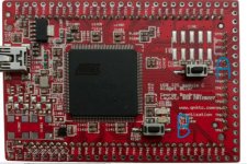
Another small question, if possible: what's the meaning of the two (red and green) small leds next to the CPU?
I suppose they are a sort of feedback about how much full are the sample buffers, but what's exactly the meaning and should they be lit or not during normal playback?
Thank you again for all your support.
thank you for your replies, the clarifications are very useful.
So, if I understand well, the CPU is running from the clock on OSC0 (connected to a 12 Mhz quartz) and so it's independent from the selected audio clock.
Is the CPU running at full speed all the time ( 66 Mhz)?
I was trying to understand if there was a change in temperature of the chip with different audio sample rates, and my impression was that temperature was invariant.
Another small question, if possible: what's the meaning of the two (red and green) small leds next to the CPU?
I suppose they are a sort of feedback about how much full are the sample buffers, but what's exactly the meaning and should they be lit or not during normal playback?
Thank you again for all your support.
1. The cpu is at 66Mhz after statup
2 the red and.green.leds toggle when the feedback rate is increased or decreased respectively. They shpuld blink when u first playback atba particular sampling rate and after a few milliseconds to seconds (depending on the clock discrepency between the host usb and the widger XO), settle to a locked atate, where one if the leds will.blink once every minute or so.
Alex
Thank you again, Alex.
Sometimes on my board at 96Khz, or 192 khz, I have both leds on .... Sometimes they change, maybe initially all off, but I got several times in the situation of both ON ... Is this normal?
Audio seems OK, no audible gaps or distortions ...
Sometimes on my board at 96Khz, or 192 khz, I have both leds on .... Sometimes they change, maybe initially all off, but I got several times in the situation of both ON ... Is this normal?
Audio seems OK, no audible gaps or distortions ...
Yes normal. As I said, the led's TOGGLE. So sometimes both are toggled to the on state (both on) and sometimes both are toggled to the off state (both off) etc.
Alex
Alex
In fact, there is another subtle effect. High jitter in the i2s clocks, especially if it is uncorrelated, may have a "spread spectrum" effect such that there may be a reduction of radiated noise from the uC side to the analog circuitry in the DAC side.
I'm glad that you mentioned spread spectrum. I see many new clock generator chips that purposefully create jitter with the goal of reducing the amount of interference at the clock frequency by spreading the spectrum, such that there is a much lower power spike at the center frequency. This is great for non-audio clocks, because it reduces interference with other electronics that might be nearby.My hunch is that for some DAC's, the MCLK is the key. The i2s is just for transferring the data across, and jitter in the i2s clocks does not impair SQ (and in fact may improve SQ because of the spread spectrum effect).
Alex
What I wonder is how you can mix spread spectrum clocks with a low-jitter audio sample clock. How do you prevent the data from getting behind the clock? As I understand it, the data must be sent (slightly) ahead of the clock so that random variations in propagation delay over different serial lines (4-wire, etc) do not cause problems. When the clock latches the data, you don't want indeterminate data.
Can you explain how spread spectrum clocks can be used in a digital audio system where a low-jitter clock is being used as the master? (and I hope this isn't off-topic for the Audio Widget)
1. The spreadspectrum clocks, SICK and LRCK, amd the SDATA, are all gemerated by the SSC in the Atmel chip and if u read the Atmel reference docs u can see they conform to i2s requiremts.
2. The jitter will be introduced by the opto/magneto isolater and internal dividers/plls of the Atmel chip.
3. The low jitter MCLK goes to the DAC direct. It is not used for clocking SDATA.
Alex
2. The jitter will be introduced by the opto/magneto isolater and internal dividers/plls of the Atmel chip.
3. The low jitter MCLK goes to the DAC direct. It is not used for clocking SDATA.
Alex
There are usually some requirements that clocks are synchronous. As long as setup times are consistenst a few ns in delay variance is a good thing. But it may make sense to look at the clock signals in a scope to see if there is a danger of signals arriving too early or too late for the edge which latches it.
In digital design, using two D-flip-flops in series is a common way to cross clock domains. The flip-flops are then clocked by the clock of the destination.
But in our case tings are synchronous. We just need to make sure that hold and setup times are within spec. I'm travelling right now, so i can't scope this myself now. I'm tempted to get a few isolators and start playing with them. We can still test propagation delays by inserting the isolators without having to actually separate the supply domains.
Børge
Has anybody had success with installing Nikolay's drivers on non-English XP? I'm stuck with a Norwegian installation. In UAC1 I'm able to follow the instructions and run Widget-Control.exe. In UAC2 the yellow question mark comes up in Devmgr. It then does not find relevant hardware in the .inf file.
Børge
Børge
Hi Borge,
are you sure that language pack has something to do with this problem ? I had similar issue when installing Nikolay's driver on english XP per his guide. When doing driver update, the list from Audio-Widget.inf was empty. Hit back, select "Don't search I will choose driver to install" (or whatever that sounds in Norwegian🙂), next and Audio-Widged was in the list.
Hope this helps.
P.S. Playback on XP (sp3 and all latest updates) with higher bitrates (192k,96k) was terrible. Frequent drop outs and metal affects every 2 to 10 seconds without any other active processes on background. Same thing with Thesycon drivers. Don't know if it was some specific problem with my hw, but after clean install of Win7 same machine plays ok, although random dropouts and "metal effects" do pop out, but only at heavy/medium cpu and hdd utilization. Well... windoze was never a real time os.
OK, I will try again. Found an old computer with a US SP3 installation of XP.
What I'm trying to do here is to simplify the test procedure for the AB-1.2 manufacturing and make sure both crystals do what they are supposed to. So today I created two wav files at 44.1 and 48 using Octave. They both play 1s 1kHz left, then 1s 2kHz right. So the two should sound the same to the test guys but play using different oscillators. That worked well with XP and UAC1.
Børge
Borges your USB-I2S device support Windows Vista? if yes wich software have I to download & where can I download? have I to install Xtals & more components to connect to Twisted Pear Sidecar?
About the lights behavior: when I plug the mini USB to the DAC, first comes the red light then the red one. In 5 seconds or so the turn off in the same order, first red then green. Noise is still there.Juanito,
Here are some questions which may help to sort things out:
- Are you using an updated firmware version?
- Are you using UAC1 (green front light) or UAC2 (red)?
- If you open up the case, how do the red and green LEDs on the module behave?
I had similar problems a long time ago on previous firmware. In that case the module LEDs started acting up a little while before the audio imperfections started.
Børge
By the way I tried the USB DAC with EXOPC tablet. Works wonderful. The Tablet it's just a pc netbook with touch screen. I't very handy because it has two USB, so you can use simultaneously the DAC and Hard drive where I store my Flacs.
I curious about the Ipad and the usb camera kit: will that work?
you may get the option with XOs (and related parts) already mounted, see: Q N K T C USB-I2S Module and Analog Boardhave I to install Xtals & more components to connect to Twisted Pear Sidecar?
- Home
- Source & Line
- Digital Source
- Open-source USB interface: Audio Widget