ceharden said:Has anyone else tried using Jim Thomsons loop gain probe?
I've inserted it into my circuit but when I run the simulation I get an invalid command error. I don't know enough about PSpice to debug it.
I don't know either, as I'm not a PSPICE person. If you have access to usenet, Jim is a regular poster on sci.electronics.cad, so you might try posting a message there.
G.Kleinschmidt said:
Is this with standard Miller compensation?
If so;
At HF, when the VAS is operating with 100% negative feedback (Cdom = short circuit) the impedance looking into the base will be (approximately) equal to the emitter resistance. In other words, the higher the emitter degeneration applied to the VAS, the greater the minimum input impedance.
The voltage gain of the VAS will be unity and the voltage gain of the LTP will be equal to the input impedance of the VAS / the gm of the LTP. At this point, Cdom cannot reduce the open loop gain of the amplifier any further.
If the gm of the LTP is great enough (compared to the minimum input impedance of the VAS), it is possible that the open loop gain may plateau at a value close to the closed loop gain. If this is the case then you will never get an adequate gain margin for stability, even if you make Cdom 100nF.
This is a danger of applying excessive emitter degeneration to the VAS.
Hi Glen,
You make a good point. I think you are referring to the Right-Half-Plane zero that one gets in such a simple Miller integrator. Indeed, if that is what you are referring to, the unity-gain signal sneak-through of the VAS actually ends up having the wrong polarity; it is non-inverting instead of the usual inverting. The RHP zero can be eliminated by placing a small resistor is series with Cm whose value is greater than 1/gm of the VAS (typically on the order of the value of the VAS emitter degeneration resistor).
If one uses a still larger value of series resistance, one gets a normal LHP zero in the open-loop response which, if used judiciously, can improve stability.
6 dB of gain margin is usually considered adequate as long as one has good phase margin. If the open-loop gain is still rolling off at 6 dB/octave for an octave above gain crossover (meaning most phase lag beyond 90 degrees is excess phase contributed by multiple far-out poles), then a gain margin of 6 dB means one can double the open-loop gain across the board and be just barely stable, at a new gain crossover frequency of twice the original gain crossover frequency.
In very rough terms, 6 dB of gain margin also means that you can cut the Miller capacitance in half and still be barely stable (assuming that your Miller integrator is still acting like an ideal integrator in the vicinity of the gain crossover frequency).
Cheers,
Bob
This is good! I was hoping this would stimulate some good discussion of the subject.
Just had a play with a 10R in series with the miller cap and there is a dB or so improvement in the gain margin. I still can't increase the VAS degeneration above about 10R before the gain margin drops to under 6dB.
The other thing I've just tried is reducing the value of R5 in the VAS CFP to 220R. Increasing the current through Q8 has also brought some small improvement. There is a limit to how far I can reduce it before loosing the benefit of minimal loading on the LTP.
Then I tried moving the integration network (C2,R30) back to beng round the whole VAS CFP and got a big surprise. Things suddenly look even better. What is very interesting is that the phase, rather than falling off like the gain, it returns to 90deg after barely reaching 180deg. If the results are to be believed I'm up to 100deg phase margin and 12dB gain margin.
See bode plot http://www.chaudio.co.uk/AmpDesign/TestAmp2Bode4.pdf
And corresponding schematic http://www.chaudio.co.uk/AmpDesign/TestAmp2Sch4.pdf
However given that I haven't managed to get the loop gain probe to work, we're still not looking at the actual loop gain, just amplifiers overall response. I don't have easy access to usenet so contacting James Thomson will have to be done by another method.
ceharden said:I don't have easy access to usenet so contacting James Thomson will have to be done by another method.
What you are calling the gain and phase margins are not actually the gain and phase margins. The gain and phase margins are defined in terms of the loop gain, not the closed-loop gain.
There's an email link for Jim Thompson at his web site.
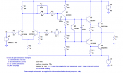
Meanwhile, there is an approximate way to simulate the loop gain, which appears in the LTspice example called "audioamp.asc". I've posted the relevant schematic below, which also has instructions on how to do the simulation.
Edit: I think you'll want to plot -V(A)/V(B) here, so the phase approaches zero as you approach DC. Put the voltage source in the same place as in the schematic, that is, from output to feedback resistor, with the nodes "A" and "B" defined as in the figure.
Attachments
If you want to reduce VAS gain, try putting a resistor (in the region of 1M) in parallel to the Miller capacitor.
Cheers Andy. I guess I should have tried that method a lot earlier in my investigations.
The resulting plot is here: http://www.chaudio.co.uk/AmpDesign/TestAmp2Bode5.pdf
I did see the email address but I wasn't sure whether I came under the category of 'student' and that meant he wouldn't appreciate such questions via email. I then wasted a good half hour trying to get onto usenet.
The resulting plot is here: http://www.chaudio.co.uk/AmpDesign/TestAmp2Bode5.pdf
I did see the email address but I wasn't sure whether I came under the category of 'student' and that meant he wouldn't appreciate such questions via email. I then wasted a good half hour trying to get onto usenet.
As if I hadn't already posted enough this evening
Well.... now I've finally got off my **** and started simulating the right thing, I'm getting some sensible results. According to the proper loopgain simulations, albeit by the crude method, all I need is a 10pF miller cap around the VAS and nothing else to get me 60deg of phase margin and 16dB of gain margin. Amp is actually far far more stable than I had thought by looking at the wrong plots!!!
Sorry for wasting everybody's time by insisting on simulating the wrong thing!
ceharden said:
I'm sorry, I don't understand the question. On my latest revision, the 22pF is replaced with a 47pF with a 1k resistor in series. The purpose of it is to further reduce the HF response but without using a huge miller cap.
Why limiting the frequency response, the output stage was oscillating?
Try to simulate a simple circuit, in general the capacitor short circuit ratio is added after, looking for square wave...
The reason for adding it was that I was looking at the wrong gain/phase plot and wrongly thinking that my amp was close to being unstable.
I have now removed that capacitor until I find out whether it is actually necessary or not.
I have now removed that capacitor until I find out whether it is actually necessary or not.
I think I've spent too long staring at simulations this evening. Have actually forgotten what I was aiming for! Time to call it a night. Good progress though. Thanks to all for their input so far.
with simulation of square wave, the oscillation show whether it is or not necessary.ceharden said:
I have now removed that capacitor until I find out whether it is actually necessary or not.
Pspice error
Did you ever get an answer for this error?
David.
Has anyone else tried using Jim Thomsons loop gain probe?
I've inserted it into my circuit but when I run the simulation I get an invalid command error. I don't know enough about PSpice to debug it.
The output I get is:
Code:.subckt SCHEMATIC1_U1 pin1 pin2 ****************** * LOOPGAIN CHECKER .PARAM PASS=0 .STEP PARAM PASS LIST 0 1 ---------$ ERROR -- Command invalid in subcircuit IMAC 0 LG AC {PASS} VMAC LG pin1 AC {1-PASS} VDUMU1 LG pin2 0 ****************** ** Copyright by James E. Thompson, 1994-2005 ** ****************** .ends SCHEMATIC1_U1
That didn't work well how about:
.subckt SCHEMATIC1_U1 pin1 pin2
******************
* LOOPGAIN CHECKER
.PARAM PASS=0
.STEP PARAM PASS LIST 0 1
---------$
ERROR -- Command invalid in subcircuit
IMAC 0 LG AC {PASS}
VMAC LG pin1 AC {1-PASS}
VDUMU1 LG pin2 0
******************
** Copyright by James E. Thompson, 1994-2005 **
******************
.ends SCHEMATIC1_U1
Did you ever get an answer for this error?
David.
No, I never did solve it. I just use a voltage source in series with the feedback. Might not be the most accurate way to do the loop gain/phase but seems to give good enough results.
Last edited:
In this test with the voltage source in series is this giving us the open loop gain or loop gain?
David.
David.
Hi ceharden,
I sent a email to Mr Thompson and just got this reply.
You need this...
[SUBCKT SETTING]
CreateSubcktForMultDevice=no
in PSpice.ini
David.
I sent a email to Mr Thompson and just got this reply.
You need this...
[SUBCKT SETTING]
CreateSubcktForMultDevice=no
in PSpice.ini
David.
I think this gives the voltage loop gain.In this test with the voltage source in series is this giving us the open loop gain or loop gain?
David.
Towards the end this thread became quite informative.
I don't get to read about the right halfplane zero too often. But Bob Cordell covered it pretty good in post 42.
When I started with (diy) amp design, I also fell for the open loop gain trap, as I tried to determine wether my design was stable by looking at the open loop gain instead of at the loop gain. As a result I got heavily overcompensated amps.
By now I use the middlebrook method to determine the loop gain, and so far it served me well.
Sometimes my approach can be a little enerving, because every change has to be done twice, as the circuit has to be duplicated to determine both the voltage- and the current-loop-gain at the same time.
I attached an LTSpice demo file.
An externally hosted image should be here but it was not working when we last tested it.
sorry for the black bar at the bottom. A bug in my screencapture program. However the most important parts are still visible.
I think I will look out for a loopgain probe for LTSpice to make things easier.
Keep up gathering valuable info on the topic in this thread.
Attachments
I think this gives the voltage loop gain.
I think I will look out for a loopgain probe for LTSpice to make things easier.
Keep up gathering valuable info on the topic in this thread.
Can you declare variables in LTspice? If you can then you could assign the same variable to the value of the component for each side. This way you would only have to change the variable value.
David.
Can you declare variables in LTspice? If you can then you could assign the same variable to the value of the component for each side. This way you would only have to change the variable value.
David.
Thanks.
I will research how to do that.
I'm quite sure this should be possible in LTSpice, if it is possible in Spice in general, wich I think it is.
I wonder if it is also possible to assign a transistor model to several devices in this way.
Thanks.
I wonder if it is also possible to assign a transistor model to several devices in this way.
If you make up an alias name for the transistor type like Trxxxx or something else, then you can just replace the model data in the .lib file for that alias and the transistor will be changed for all using that alias.
David.
Overall feedback vs. local feedback and reserve gain
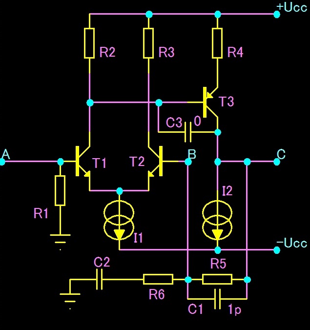
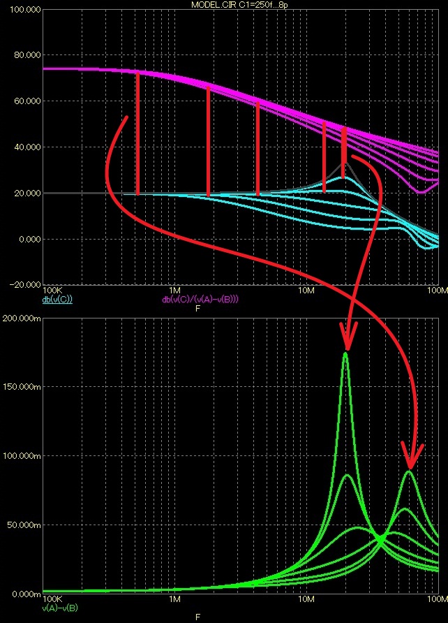
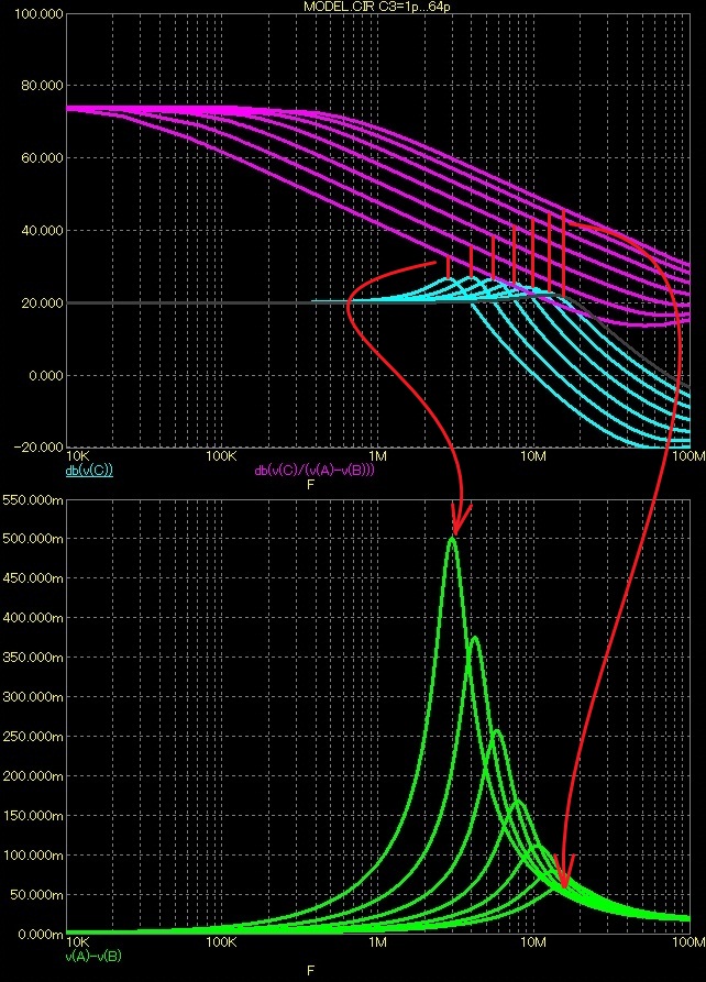
For many years I deal with the same problem. Maybe it helps.
Nice day
- Status
- Not open for further replies.
- Home
- Amplifiers
- Solid State
- Open loop gain, phase margin etc