I've been searching but there doesn't seem to be any definitive answers or reference to some of the basic issues of amplifier design/optimisation. I'm hoping by posting some of my investigations we can create a reference for other people looking for the same information.
I've gone back to basics with my amplifier design. I have a prototype running but decided before I transfer it to PCB to effectively start again and go through the whole design progress. While my current design works (amp listening to the one prototype channel at the moment) I think there is improvement to be made, especially regarding stability. Doesn't like 100kHz square wave test signals for some reason! 😀 Going back to the simulations suggest that the phase margin is fairly non-existent which would explain why it was a PITA to compensate.
So, I'm just looking at the LTP and VAS at the moment. I'm playing with this circuit and a bode plot is shown here
My observations so far are that I've got a fairly decent amount of open-loop gain, even with the quite large emitter degeneration resistors in the LTP. As expected, these resistors improve the phase margin significantly. What surprised me however was that adding degeneration to the VAS actually degraded the phase margin.
My main questions are, how much open loop gain do I need? I intend the final amplifier to have a closed loop gain of either 26dB or 32dB (20x or 40x). How much phase margin is acceptable, good etc? The circuit shown has about 60deg of phase margin.
I'm currently using the crude large inductor and capactitor method of calculating open-loop gain. Is this accurate enough for what I'm doing?
I look forward to a good discussion about this!
Chris
My main questions are, how much open loop gain do I need?
How many negative feedback do you want to apply?
That is, I'm sorry, at the heart of designing an amp. Effectively there are 2 different companies here in this forum: low OLG, low NFB, rather high THD or the same in high (with THD low 😉 ).
Plenty of room in between.
Have fun, Hannes
Thanks for the reply. I am aware that there is some difference of opinion on the subject but I'm trying to put some figures to the descriptions.
What is regarded as low NFB? 10dB? 30dB? What is high NFB? 40dB? 60dB?
My application is for things like studio monitors so I'm looking for accuracy and neutral sound. I would imagine that would put me into the high NFB camp. From my simulations so far, I would expect that I'm likely to get somewhere in the region of 50dB NFB (80dB OLG - 30dB CLG). Is this reasonable?
so I'm looking for accuracy and neutral sound.
Don't we all 😀
Your NFB number might be ok, depending on exact topology and all other design choices.
Why don't you save yourself all the trouble and build a proven low distortion amp like one of Douglas Self's amps? Search for 'blameless' - or better buy his book 😉
I wouldn't trust distortion figures from simulation in general - but that depends very much on your own SPICE-knowledge and experience with device models. You can easily end up with an amp that measures far worse than simulated.
Have fun, Hannes
There's no challenge in building somebody elses design for me. I look at them for inspiration but I won't copy wholesale. Part of the whole point of this for me is to learn how to design them and I find the best way is to do it! I design my own speakers, so I want an amplifier I've designed myself to go with them!
Yeah, I perfectly understand 😀
That's the hard part if you want to do a high NFB-design properly. I really recommend to get Self's book on Audio amp design, you will learn a lot on the sources of distortion. Indispensable in my opinion for serious low-THD designs.
For a low THD-amp, it's essential to verify performance. Get/setup a decent soundcard and a low THD-oscillator for measurement. Be prepared to build a number of prototypes that probably will disappoint you in comparison to simulation.
Hey, but it's a lot of fun!
Have fun, Hannes
PS: by the way, have a look at Grey's GR-25 amp; folded cascode topology with pretty little distortion and low feedback - see it's possible 😉 It just depends on what is your target.
learn how to design them
That's the hard part if you want to do a high NFB-design properly. I really recommend to get Self's book on Audio amp design, you will learn a lot on the sources of distortion. Indispensable in my opinion for serious low-THD designs.
For a low THD-amp, it's essential to verify performance. Get/setup a decent soundcard and a low THD-oscillator for measurement. Be prepared to build a number of prototypes that probably will disappoint you in comparison to simulation.
Hey, but it's a lot of fun!
Have fun, Hannes
PS: by the way, have a look at Grey's GR-25 amp; folded cascode topology with pretty little distortion and low feedback - see it's possible 😉 It just depends on what is your target.
30dB of feedback at 20kHz is typical. Much more than that and stability becomes troublesome.
90 degrees of phase margin is ideal. 60 degrees should be fine. 30 degrees is low.
Even an amplifier with plenty of phase margin can have stability problems due to its inductive output impedance, so don't omit a Zobel network on the output. Additionally, an output inductor helps with stability into capacitive loads.
Originally posted by h_a PS: by the way, have a look at Grey's GR-25 amp; folded cascode topology with pretty little distortion and low feedback - see it's possible 😉 It just depends on what is your target. [/B]
Isn't Greys GR-25 with NO feedback?
Ok, thanks for the info. I'm heading along the right lines it seems.
Here's schematic of what I think is a fairly realistic input/VAS stage for my amplifier:
http://www.chaudio.co.uk/AmpDesign/TestAmp2Sch1.pdf
Spec's:
LTP bias current: 2.2mA/leg
VAS bias current: 8mA
Maximum OLG = 103dB
Open Loop phase margin = 60deg
Closed Loop (gain = 20x/26dB) phase margin = 50deg
Response -3dB @ 750KHz
Now obviously the frequency response extends somewhat higher than needed and would probably oscillate freely if built as such. What -3dB frequency is reasonable? I'm thinking 50kHz maybe? Should I control that using more VAS miller compensation or a small cap across the feedback resistor seems to do the trick?
There are many ways to compensate an amplifier. I will mention just briefly some of them.
The most common one and very easy to implement is one pole compensation, also called dominant pole compensation, just like you are using. The drawback of this type of compensation is that it sets a pole in transfer function at very low frequency (in range 10Hz to several kilohertz) where the OLG begins to continuously drop 20dB/dec which gives you very low OLG at higher frequencies. Capacitor used is in range of few pF to 100pF. You can also achieve this kind of compensation by tying capacitor between VAS and ground. D.Self calls this a crude way of compensation.
Second also common method of compensating an amplifier seen here is by loading the VAS with a resistor (10 kilohm's and more) to the ground. I have seen some professional designs using this method.
Compensation using zero and pole, known as LAG compensation, can give you more OLG bandwidth and increase OLG at higher frequencies. This allows to get some nice THD numbers, but unfortunately this type of compensation degrades dynamic performances of an amplifier. This type of compensation is achieved by putting a resistor ( few hundred ohms to kilohm) in series with a capacitor (100pF to several nF) to ground or +/-Vcc depending on topology.
Very often you will see a small capacitor (few pF) in parallel with upper feedback resistor. This is called LEAD compensation and it is often used in combination with some other compensation to improve phase margin. It also improves amplifier response times. If you put to big capacitor here, then you can degrade phase margin so use this carefully.
Of course, you can combine these compensations to achieve what you want.
I'm not an native English speaker, so...sorry for any mistakes.
More useful info. Some I knew about but good to have it confirmed.
At the moment I'm using 47pF for both the Miller Compensation and Lead compensation across the feedback resistor. Those two together are giving me a really good closed loop phase margin (130deg) but the response is still only just starting to tail at 100kHz which still seems a little high. Trying to reduce the bandwidth further seems to do more harm than good.
Next step I guess is to add the output stage and see what nastiness that introduces!
Can you post a picture of open loop response or transfer function? I'm not sure if I am following you right. 🙁 (different terms, but the same thing). 130deg of phase margin seems a bit high (but good nevertheless), what is the gain margin (gain at 180 deg)?
If you are going to use BJTs than I suggest using emitter follower configuration.
If you are going to use BJTs than I suggest using emitter follower configuration.
Will post pics in a bit but I'm having a play with the open loop (no NFB) and closed loop (with NFB) responses. The best I can get open loop is about 60deg of phase margin and that's just with the VAS Miller compensation. The lead compensation capacitor doesn't help or makes things worse.
In the closed loop situation, the lead comp capacitor is very useful to optimise the response. However if I then re-simulate the open loop response with the same component values, I get a very poor phase margin.
Should I be optimising the phase margin for open loop or closed loop response?
In the closed loop situation, the lead comp capacitor is very useful to optimise the response. However if I then re-simulate the open loop response with the same component values, I get a very poor phase margin.
Should I be optimising the phase margin for open loop or closed loop response?
Do you run a real amplifier open loop or closed loop?ceharden said:...Should I be optimising the phase margin for open loop or closed loop response?
Mr Evil said:
Do you run a real amplifier open loop or closed loop?
Yea, a good question...

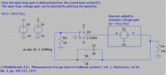
And here is another way of OLG simulation.
Attachments
When you put it like that.....
There's so much said on here about open loop response you do wonder which is more important!
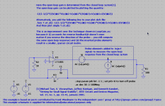
Plot of response with NFB applied is here: http://www.chaudio.co.uk/AmpDesign/TestAmp2Bode1.pdf
In that case the Miller comp was 47pF and the lead comp 33pF
Circuit diagram has been updated too: http://www.chaudio.co.uk/AmpDesign/TestAmp2Sch1.pdf
There's so much said on here about open loop response you do wonder which is more important!
Plot of response with NFB applied is here: http://www.chaudio.co.uk/AmpDesign/TestAmp2Bode1.pdf
In that case the Miller comp was 47pF and the lead comp 33pF
Circuit diagram has been updated too: http://www.chaudio.co.uk/AmpDesign/TestAmp2Sch1.pdf
Whole amplifier - sanity check required
Right, I've added an output stage to my input/VAS stage and tweaked to get some kind of phase margin etc.
I looked at various output stages but for some reason settled on the one in my current prototype (except the biassing).
Schematic is here : http://www.chaudio.co.uk/AmpDesign/TestAmp2Sch2.pdf
Bode plot of amp: http://www.chaudio.co.uk/AmpDesign/TestAmp2Bode2.pdf
I'm curious as to what causes the little lump in the response. It seems to be at one of the poles. The phase margin is good at about 90deg but that little kink reduces the gain margin to only a few dB.
Wanted to do a distortion simulation but the results say no distortion so something must be wrong! Need to look at that further.
So I've basically ended up at the schematic I had before doing all the analysis. What I actually built is very close to http://www.chaudio.co.uk/AmpDesign/Amp1SchProtoReady.pdf
Any comments appreciated!
Chris
you mentioned in your original post that your amp doesn't "like" 100khz square waves...... could you be more specific? does it do something like oscillate at 1Mhz, or does it just draw tons of current with no load? if the problem is oscillation, then you should be looking for compensation problems, or slew rate mismatches. if it's a huge current draw, then it's likely you are having problems with common mode conduction (also known by other names like "bleed through, punch through", etc....). what it boils down to is the + half outputs and/or the - half outputs are still conducting while the other half begins conducting, so you have huge currents flowing from one supply rail to the other. the reson for this is that the capacitance of the B-C junction requires a finite time to discharge, and the current to cause this isn't high enough. so the transistor remains in the conduction state longer than it should. the solution to this is a lower impedance path between bases of the output devices, and higher currents for the drivers.
a good paper on what i mentioned above called "slew rate mismatch" is available in one of the appendices of Linear Technology's AN47 application note about high speed amplifiers. apparently if your input stage is very fast, and your output stage is slow, it adversely affects the phase margin. it's better to slow down the input stage (easy) or speed up the output stage (not so easy).
a good paper on what i mentioned above called "slew rate mismatch" is available in one of the appendices of Linear Technology's AN47 application note about high speed amplifiers. apparently if your input stage is very fast, and your output stage is slow, it adversely affects the phase margin. it's better to slow down the input stage (easy) or speed up the output stage (not so easy).
You might want to take a closer look at Q20...
If that lump is causing you trouble, try adding a zero to cancel a pole. You can do that by putting a resistor in series with C3.
If that lump is causing you trouble, try adding a zero to cancel a pole. You can do that by putting a resistor in series with C3.
- Status
- Not open for further replies.
- Home
- Amplifiers
- Solid State
- Open loop gain, phase margin etc