Christian try postimage.org
I use it 24/7 and i love it. Got a gallery there too... Postimage.org / ... 😛
Gerald, nice schematic indeed... I ll talk aboutmy ideas later, its almost midnight 🙁
I use it 24/7 and i love it. Got a gallery there too... Postimage.org / ... 😛
Gerald, nice schematic indeed... I ll talk aboutmy ideas later, its almost midnight 🙁
Last edited:
Gerald,
Yours is pleasurably simpler. And I don't even know that one couldn't get away with even less. How well did it work?
Yours is pleasurably simpler. And I don't even know that one couldn't get away with even less. How well did it work?
It worked great it is a classic configuration from National Semiconductor from many years ago !!
I will be working with it again soon and show some Scope test's.
At the moment I have been in repair mode fixing and re-arranging monitors and setting up another machine for some PIC programming.
Once my bench is cleared off again, I will be getting in to testing the new opamp samples that I have been collecting for the last 6 months.
jer 🙂
Last edited:
Hey I remebeber this circuit few years ago when i started the whole electronics thingy..
in that circuit theres a transistor used as bias? I mean like your can use a lot smaller trimmer pot... but even with to220 transistors its pretty much impossible to turn your trimmer into a smoker.
in that circuit theres a transistor used as bias? I mean like your can use a lot smaller trimmer pot... but even with to220 transistors its pretty much impossible to turn your trimmer into a smoker.
Fu** those TO3s aint gona waste my time on them!
My biasing circuit is missing, I really want to keep it simple, so what about Geralds one?
Theres also missing HF caps on the opamps rails
Going to use 4X 1W 1R resistors as I was unable to find better solution... those giant 5W axials are available everywhere
AAAAAAAARGHHHHHHHHHH!!!!!!!!! what the fail, dat aint cool,I got 8 more resistors to place.
Last edited:
Looks like TI aint gona give meh my samples ey 🙁 None of them are available...
But anyway 14€ should be fair price... 2 pcs... When i burn one I may be very upset.
But heya I think i made something... Bias is as simple as it can be... Probably too simple and it will start smoking which can make me smoke again....
I could have made a lot better one...
But here it is :
photo hosting
But anyway 14€ should be fair price... 2 pcs... When i burn one I may be very upset.
But heya I think i made something... Bias is as simple as it can be... Probably too simple and it will start smoking which can make me smoke again....
I could have made a lot better one...
But here it is :
An externally hosted image should be here but it was not working when we last tested it.
photo hosting
Last edited:
I started an answer for you last night, But I hit the back button and lost the whole mess!!!
The value of the pot was just something that I had laying around and I have not taken the time to find the optimum value.
It does give me a range to work with down to zero and the resistors are what set the actual high current limit.
I was able to get up into the 2 to 3 amp range per device using my unregulated 26v single ended supply.
But as expected the voltage swing was limited.
I didn't want to go much over 1.5 amps with the test as they got rather warm.
The Pd of the BD911/912's are at only 90 watts that was good until I build a version with more of them paralleled.
Due to the very high current gain (Hfe) of the darlington configuration, I figured that only about 5 to 10ma. is all that is required to send the output devices well into and past their Pd limit.
Yes, working with TO-3 packages is a PIA when it comes to PCB design.
In such cases I just use wires from the PCB to connect them, this way it does not matter in which order they are on the board.
I did start a board design with this circuit but I haven't finalized it yet because I don't know how many output devices I will be using yet.
I do plan to have a bridging capability iincorporated in the circuit as well for higher power operation with single ended high current supply's, since I have plenty of them in the 20 to 30 volt range.
jer 🙂
P.S. I just received my LME49720's that have been on backorder since July !!! 🙂
Nice board layout as I just saw it after making this post!!!🙂
Although, I can't tell if there are any mistakes yet, what schematic are you using?
Last edited:
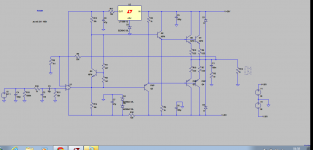
Not sure is this board is finished but looks pretty good to me...
Iam not sure how does the biasing work... on both SCHs im just lost, just today, maybe tomorrow I get it.
I will use PCB rivets in 1,5mm+ holes Dont have any smaller ones in hands, cant get them anywhere near too :/
Input of the opamp is missing :O The opamp side is messed up right now, I first tried 3 hours on single layer, too many jumpers... too unbalanced...
Then with 2 layer design I first made few mistakes but seems alright for today...
I may make a little copper shielding for the opamp to keep noises away... I got some copper sheet metal, around 0.15-0.2mm in thickness. Ill be back 🙂
But top and bottom layers.. :
image hosting
image hosting 10mb limit
Iam not sure how does the biasing work... on both SCHs im just lost, just today, maybe tomorrow I get it.
I will use PCB rivets in 1,5mm+ holes Dont have any smaller ones in hands, cant get them anywhere near too :/
Input of the opamp is missing :O The opamp side is messed up right now, I first tried 3 hours on single layer, too many jumpers... too unbalanced...
Then with 2 layer design I first made few mistakes but seems alright for today...
I may make a little copper shielding for the opamp to keep noises away... I got some copper sheet metal, around 0.15-0.2mm in thickness. Ill be back 🙂
But top and bottom layers.. :
An externally hosted image should be here but it was not working when we last tested it.
image hosting
An externally hosted image should be here but it was not working when we last tested it.
image hosting 10mb limit
Last edited:
The way the biasing works is actually very simple. We know that we have one diode drop from base to emitter, 1 x Vbe, so we know the current down that arm (the one with the other resistor in it, or resistor and pot) so we know that the voltage across that resistor will be proportional to its value x 1 Vbe. So if it is 3 times the value, you will get 3 times the drop across it, making 4 Vbe drops in all.
The way this ends up as bias current is that it pushes the bases of the two transistors apart, so increasing the voltage across their emitters and turning them on more.
It is interesting to mention that collapsing the bias is one method often used to protect an amplifier or speakers in fault condition. If there is no voltage across the emitters then there will be no conduction. It doesn't tend to work very well in practice but it could save your transistors in a short. Quite a number of 70s amps had it.
Incidentally I did reply to you earlier, but the msg seems to have got lost.
But I should mention (again) that if you do it with just diodes, which will work fine, then you won't be able to adjust the bias, let alone push it properly into Class A. So the Vbe multiplier is your simplest option for that.
What I said on the missing reply was that the problem with the schematic I'd put up was that you only get 30dB of power supply rejection due to R13 and R14 and that at least an RC, or a zener would be needed to bring this down. Ideally you'd regulate it properly and get 70dB on the lines plus the 30dB you had. There's oodles of voltage to play with so something like a couple of 20V zeners, preferably feeding a pass transistor, should see you through.
I hope you follow that.
I hope you follow that.
Not sure I follow this board at all and I'm very uncertain about putting pnps at one end and npns at the other. You need to be able to follow the temperature, and you only have one transistor to do that with (the one in the Vbe multiplier) and you have to keep them all at the same temperature or their conduction will be different. I imagine that will show up as a DC offset.
But I do like the idea of paralleled output transistors (or is this trying to be stereo) and paralleled REs is a good idea too. If you are doing paralleled output transistors then you will need emitter resistors for both sets, not one resistor (albeit paralleled) doing both transistors. This helps hugely with current sharing between the devices.
Unfortunately it's a bit late or I'd knock this up on LTspice. (Which you must get a copy of - just google it).
BTW, what software are you using for your boards? And is it easy to use?
With these mistakes it is unreadable.. .
Now the transistors, power supply, bias...... seem fine to me...
Im not sure yet... Im still lost but thanks ALOT GeraldFryJR AND ChristianThomas!
You guys are amazing, truly master teachers. Christian has made half of the posts in this thread, wow.
Gerald, congratiolations on receiving your devices!
LTSpice, holy ****. I never knew there were similar software out there for free :O
Anyway, the PCB software I use is ExpressPCB that is pretty basic...
But I can make toutorial for it if needed... Many many things you can do with it, Its not that basic when you know how to use it, Its pretty much limitless but yet theres better ones out there
image hosting sites
jpg images
Now the transistors, power supply, bias...... seem fine to me...
Im not sure yet... Im still lost but thanks ALOT GeraldFryJR AND ChristianThomas!
You guys are amazing, truly master teachers. Christian has made half of the posts in this thread, wow.
Gerald, congratiolations on receiving your devices!
LTSpice, holy ****. I never knew there were similar software out there for free :O
Anyway, the PCB software I use is ExpressPCB that is pretty basic...
But I can make toutorial for it if needed... Many many things you can do with it, Its not that basic when you know how to use it, Its pretty much limitless but yet theres better ones out there
An externally hosted image should be here but it was not working when we last tested it.
image hosting sites
An externally hosted image should be here but it was not working when we last tested it.
jpg images
Last edited:
Mihkus
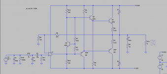
This is the sort of thing I would be aiming for.
It should all be laid out so you can't make any mistakes. I have put in a proper regulator on V+ (that can be a 317), but I don't have the model for it) or you can leave it out and just use what I have put on V- (conveniently because I don't have a model for a 337 either - at least not easily to hand), or you can leave out the zener diodes (you only need one, but the std library comes with very few so I have put in two 12Vs rather than one 24V.) Or you can leave that out too and just have a resistor and cap. Or even leave those out!
This should show you how to do the power transistors. I still say you should have all of them on the same strip of heatsink, with the Vbe transistor in the middle. So NPN, NPN, Vbe, PNP, PNP.
You do not need your 10,000 uF caps on this board. I have put in a couple of 100uF caps where they should be, near the transistors. You'll have to take a bit more care over your Ground(s). You really want the power to your op amp away from the hefty currents that will shuttle between those big caps. For all sorts of reasons. And you really need a spur to take off the main ground, rather than have it just somewhere between their + and -.
If I remember from the last time I thought about this, the way to lay out the paralleled power transistors, when they are sitting side by side, is to have track going behind the pins (imagine if they were standing up). Make those track lengths the same for each transistor, or same resistance.
I've also done a CFP version - note the change in R1 as we now have only two diode drops, approximately.
If you use something like the MJE15034/5 as your drivers, you could actually make a very simple power amp out of them alone. I have put this in as the third schematic. You could then build up from that to a CFP, from diodes to a Vbe multiplier, adding decoupling and so on. It's up to you. By and large, though, I think this is the range of your choices when doing it this way. (Well certainly for this level of complexity.)
Error - On the CFP the base of Q6 should go to the collector of Q5. There seems to be a wire missing. I lost my first effort at this for some reason, so I just lashed this up quickly.
Also note that I have used 3 diodes on the bare bones amplifier. It wasn't quite switching on with just two. This leaves it with about 150mA of quiescent, which is probably quite generous. You'll find out what it really is when and if you build it!
Attachments
Last edited:
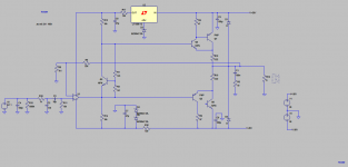
GROUNDING!!!!!!!!!!!!!!!!!!!!!!!!!!!!!!!!!!!!!!!!!!!!!!!!!!!!!!!!
What the heck, i need star grounding for keep noises away.. and to keep things stable...
I bet the resistor values are incorrect, It might even work like that but I dont know what transistors were in use in the circuit shown on page 4 post 42 by Gerald.. http://www.diyaudio.com/forums/chip-amps/244818-opamp-plus-driver-stage-output-stage-its-own-supply-what-could-happen-5.html#post3696344
Should i put caps between drivers emmiters and gnd? would it do anything better? I get noisy stuff in there...
upload pictures online
What the heck, i need star grounding for keep noises away.. and to keep things stable...
I bet the resistor values are incorrect, It might even work like that but I dont know what transistors were in use in the circuit shown on page 4 post 42 by Gerald.. http://www.diyaudio.com/forums/chip-amps/244818-opamp-plus-driver-stage-output-stage-its-own-supply-what-could-happen-5.html#post3696344
Should i put caps between drivers emmiters and gnd? would it do anything better? I get noisy stuff in there...
An externally hosted image should be here but it was not working when we last tested it.
upload pictures online
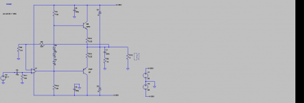
Cant change anymore damn! 🙁
But added few more traces and... seems fine to me, tired and hungry
Is there something i can do with opamp... I mean something like star grounding... But theres no high currents being drawn.. So there would be no point? The supply rails to opamp... Should i wire my opamp directly from power supply?
how to take screenshots
But added few more traces and... seems fine to me, tired and hungry
Is there something i can do with opamp... I mean something like star grounding... But theres no high currents being drawn.. So there would be no point? The supply rails to opamp... Should i wire my opamp directly from power supply?
An externally hosted image should be here but it was not working when we last tested it.
how to take screenshots
Last edited:
I've just had a quick glimpse, but don't have time to study your board thoroughly. But don't use 6.6k in the Vbe multiplier. That gives around 4A and is not the best starting point. You will not need (or perhaps be able to get to) more than 2A anyway, I shouldn't think, depending on the load you are driving. But start low, and/or put in a preset.
I will have a better look later.
I will have a better look later.
- Status
- Not open for further replies.
- Home
- Amplifiers
- Chip Amps
- opamp plus driver stage and output stage with its own supply, what could happen?