Member
Joined 2009
Paid Member
Hi Sébastien,
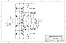
Looking at post 6, I like the approach, or at least I think I do - I’m trying to get my head around it still (I wasn’t able to access all the links your posted). So it looks like the op-amp is driving R9 causing a current flow through it’s power rails which is mirrored to provide an input signal to the power FETs.
What is the function of R6 ?
I’m not sure that I would trust the spice simulations too much because I suspect the op-amp models are rather idealized and will not be able to show up some nuances.
With the extremely wide bandwidth of the op-amp the pcb layout and stability is likely to require a lot of close attention. I agree with Mooly, it’s a promising design but you might need to build and test it to find out what things need attention that the simulations don’t show. I remember re-spinning my first MOSFET amplifier pcb design 3 times before I was happy that it was stable (TGM7).
My thought is that really low distortion is not critical for sound quality here. It might be interesting to adjust the mix of the feedback signal. Instead of taking it all from the output you could take some of it from the output of the op-amp directly. You could take all of it from the output of the op-amp and let the output stage run open-loop. The distortion would be higher, but you might like the sound, it will also be speaker-dependent and it would be a revealing experiment to try.
I know LatFETs are said not to require source resistors when they are put in parallel, but I don’t know if this is reliable in practice, somebody with more practical experience of using them would have to comment on that.
op amp macromodels can be poor - some may not even reflect the output current in their power supply pins - you do have to check with test circuits or careful reading of the model
even those that get ps pin current ~right are not using full Q models of the output stage so crossover defects, asymmetric source/sink gains probably won't be very realistic
even those that get ps pin current ~right are not using full Q models of the output stage so crossover defects, asymmetric source/sink gains probably won't be very realistic
Last edited:
I know LatFETs are said not to require source resistors when they are put in parallel, but I don’t know if this is reliable in practice, somebody with more practical experience of using them would have to comment on that.
That is true, they don't need the resistors if the devices are well matched (vgs vs Id). Think of the "double die" devices such as the Alfet ALF16N16W types.
Hi Sébastien,
Looking at post 6, I like the approach, or at least I think I do - I’m trying to get my head around it still (I wasn’t able to access all the links your posted). So it looks like the op-amp is driving R9 causing a current flow through it’s power rails which is mirrored to provide an input signal to the power FETs.
What is the function of R6 ?
I’m not sure that I would trust the spice simulations too much because I suspect the op-amp models are rather idealized and will not be able to show up some nuances.
With the extremely wide bandwidth of the op-amp the pcb layout and stability is likely to require a lot of close attention. I agree with Mooly, it’s a promising design but you might need to build and test it to find out what things need attention that the simulations don’t show. I remember re-spinning my first MOSFET amplifier pcb design 3 times before I was happy that it was stable (TGM7).
My thought is that really low distortion is not critical for sound quality here. It might be interesting to adjust the mix of the feedback signal. Instead of taking it all from the output you could take some of it from the output of the op-amp directly. You could take all of it from the output of the op-amp and let the output stage run open-loop. The distortion would be higher, but you might like the sound, it will also be speaker-dependent and it would be a revealing experiment to try.
I have in the past evaluated open loop OP stage with high bias class A
versus same stage with local FB and hence lower distortion. Front end was
the same so we were just listening to the OP stage. Subjectively open loop
has a lot going for it. The sound is big, open, relaxed, musical and engaging.
There's not much not to like 🙂
On the other side of the coin when applying feedback there was more
perceived resolution and detail. Faster transients and a feeling that this
must be technically more correct. However along with this more 'technically
correct' sound is a subjectively more washed out sound with less connection
to the music.
So for me it was always a very tricky path to find a good balance between
the two. I want something to be accurate but ultimately you have to be able
to listen to it.
I am currently working on a current feedback amplifier with moderate loop
gain, fairly reasonable OP stage bias, very small value OP stage emitter
resistors. The result is deeper class A for a given OP bias, very good
HF distortion and a fairly flat distortion curve versus frequency. It is also
very stable. I think this will subjectively be a great balance between an
amplifier that has very low distortion and one that sounds right.
I know LatFETs are said not to require source resistors when they are put in parallel, but I don’t know if this is reliable in practice, somebody with more practical experience of using them would have to comment on that.
Just match them and they will be fine sans source resistors.
cheers
T
Very interesting. Why do you use 2 pairs mosfet for +-35V powe supply? I think one pair is enough for 4 Ohm load.
Please build it...😎
Please build it...😎
I found that even with good matching (by my standards and ability) AND using accurately matched Source Resistors (0r1) that considerable variation in quiescent current is the end result of paralleling lateral mosFETs. Some will run hotter than others. Even at the higher temperatures the currents cannot match the cooler devices.
I reported these results way back.
I reported these results way back.
I found that even with good matching (by my standards and ability) AND using accurately matched Source Resistors (0r1) that considerable variation in quiescent current is the end result of paralleling lateral mosFETs. Some will run hotter than others. Even at the higher temperatures the currents cannot match the cooler devices.
I reported these results way back.
This will likely be a thermal issue. If they are well coupled thermally and you
have used HQ insulating pads, good thermal mass heatsink, there will be no
problems. It has to be so - they are relatively low gm devices.
T


HI LC
Thanks for this scheme ! I will simulate.
I just intend to try with a cascode on the VAS or in compound and possibly with a buffer before mosfet.
Maybe quasi complentary mosfet 🙂 I have more 2SK than 2SJ
What is the second cascode purpose ?
Cascode or double cascode should be better than compound ?
I found this on french forum :
An externally hosted image should be here but it was not working when we last tested it.
Last edited:
Yes, it's a Thermal issue.This will likely be a thermal issue. If they are well coupled thermally and you
have used HQ insulating pads, good thermal mass heatsink, there will be no
problems. It has to be so - they are relatively low gm devices.
T
The higher Ibias device run hotter than the lower Ibias devices.
No amount of matching overcomes that.
Omitting the Source Resistor makes the Ibias balance even worse, i.e. bigger temperature differentials between devices.
There is a big advantage to omitting the Rs, one never finds out that some devices are running much hotter than others.
No knowledge equals no concern.
Last edited:
Hi Guys
At this moment i prefer running the sim with only lateral mosfet.
I will return to the use of bipolar later
Yes at 20Khz we have 10X more distortion due to the 10X less gain ... maybe due to the HF compensation ?
However, I will I'll grant more attention and try to decrease
Yes I've seen several times on the zener mosfet as the VSSA
LC, no need ZENER with the schematic you just gave ?
What about BJT outputs? They seem to run a bit better at lower bias current...
The peformance is already impressive.
At this moment i prefer running the sim with only lateral mosfet.
I will return to the use of bipolar later
Do the sym at 20kHz and you will see that it just has truck loads of
OLG at lower frequencies with steeply rising distortion at higher frequencies.
Generally this is not a great thing for sound quality. You are better off having
a flatter distortion versus frequency curve, even at the expense of increased low freq distortion.
Yes at 20Khz we have 10X more distortion due to the 10X less gain ... maybe due to the HF compensation ?
However, I will I'll grant more attention and try to decrease
place a 5.1 volt zener where the 75 ohm resistor is. That should keep the HF distortion in check.
Yes I've seen several times on the zener mosfet as the VSSA
LC, no need ZENER with the schematic you just gave ?
10x more than nothing? - I really don't think this is a legit criticism at such low levels of distortion
we still have to deal with Otala's "contributions" to audio design debates - but not because they are objectively supported - but because audio guru's, their fanboy's still like the stories
Otala's flat loop gain over audio prescription was based on a flawed/incomplete analysis - even early "converts" Walt Jung and Marshall Leach who published "low TIM" designs came to realize you can have high feedback, sloping gain and low TIM/PM
Otala's prescription has been beaten to death in JAES, by Cordell, Cherry... in articles including analysis, practical real world amp builds, measured with custom PIM analyzer hardware
in over 30 years we still do not have acceptable psychoacoustic controlled listening test evidence for the audibility claims - only anecdotal "testimony" - by those admitting they don't listen with a Blinding protocol, other required controls
Last edited:
Hi Sébastien,
Looking at post 6, I like the approach, or at least I think I do - I’m trying to get my head around it still (I wasn’t able to access all the links your posted). So it looks like the op-amp is driving R9 causing a current flow through it’s power rails which is mirrored to provide an input signal to the power FETs.
What is the function of R6 ?
I’m not sure that I would trust the spice simulations too much because I suspect the op-amp models are rather idealized and will not be able to show up some nuances.
With the extremely wide bandwidth of the op-amp the pcb layout and stability is likely to require a lot of close attention. I agree with Mooly, it’s a promising design but you might need to build and test it to find out what things need attention that the simulations don’t show. I remember re-spinning my first MOSFET amplifier pcb design 3 times before I was happy that it was stable (TGM7).
My thought is that really low distortion is not critical for sound quality here. It might be interesting to adjust the mix of the feedback signal. Instead of taking it all from the output you could take some of it from the output of the op-amp directly. You could take all of it from the output of the op-amp and let the output stage run open-loop. The distortion would be higher, but you might like the sound, it will also be speaker-dependent and it would be a revealing experiment to try.
I know LatFETs are said not to require source resistors when they are put in parallel, but I don’t know if this is reliable in practice, somebody with more practical experience of using them would have to comment on that.
R6, R9 are buffer local feedback, but actually serves as load.
In fact you suggested me to use a local CR instead of global?
I'd like 🙂 It will come later
10x more than nothing? - I really don't think this is a legit criticism at such low levels of distortion
10x nothing on a sym with idealized opamp and other components, etc etc.
Transfer that to real life and you will likely have anywhere up 10 x 10 = 100
x HF distortion. I'm looking at the complete picture here, feet planted in the
real world.
we still have to deal with Otala's "contributions" to audio design debates - but not because they are objectively supported - but because audio guru's, their fanboy's still like the stories
Otala's flat loop gain over audio prescription was based on a flawed/incomplete analysis - even early "converts" Walt Jung and Marshall Leach who published "low TIM" designs came to realize you can have high feedback, sloping gain and low TIM/PM
Otala's prescription has been beaten to death in JAES, by Cordell, Cherry... in articles including analysis, practical real world amp builds, measured with custom PIM analyzer hardware
I don't remember promoting anything WRT Otala. From what I've seen of
those amplifiers they didn't really do anything measurement wise that looked
particularly spectacular.
I was referring to the subjective qualities of certain distortion vs freq
characteristics.
You might find it interesting that even very theoretically brilliant people such
as B Putzeys have similar views WRT the distortion versus Fr characteristics
(as far as I am aware).
T
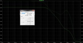
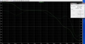
I used your LTspice file to simulate loop-gain of the amplifier. Under the current 4Ohm resistive load, the amplifier has sufficient phase margin (90 deg).
The original LTspice file modified for loop-gain measurement is attached.
The original LTspice file modified for loop-gain measurement is attached.
Attachments
Based on the circuit in post #6. The opamp is replaced by high-performance LT1128 audio opamp. Feedback resistors are changed to 1 k and 22 k to avoid heavy loading to LT1128 (low values have not tried for min. noise).
LT1363 THD
1k = 0.000071%
10k = 0.000850%
20k = 0.002485%
LT1128 THD
1k = 0.000024%
10 k = 0.001617%
20 k = 0.005159%
Let take a look of loop gain of the two circuits. LT1128 has very high loop gain in low band. On the other hand, LT1363 is a low open-loop gain wide bandwidth opamp. The circuit has a "flatter" loop gain. This explains lower THD in high band.
Loop-gain (dB) of the two amps.
(LT1363 based amp) (LT1128 based amp)
2k 62 60
3k 61 56.5
20k 52 40
30k 49 36
40k 47 34
50k 44 32
60k 43 31
LT1128 based circuit is traditional dominant pole compensated amp with a roll-off of -20 dB/decade. In contrast, LT1363 based circuit roll-off is ~10 dB.
LT1363 is a current-feedback amp with high-impedance inputs for use as a voltage amp. It combines goodies of both architectures?
Attachments
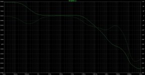

We can improve phase margin (PM) of LT1128 amp circuit by using larger output to gate caps. Example below uses 470pF to improve PM from 36 deg to 66 deg. Crossover frequency is practically unchanged.
PM of LT1363 amp is 90 deg.
PM of LT1363 amp is 90 deg.
Attachments

Based on the circuit in post #6. The opamp is replaced by high-performance LT1128 audio opamp. Feedback resistors are changed to 1 k and 22 k to avoid heavy loading to LT1128 (low values have not tried for min. noise).
LT1363 THD
1k = 0.000071%
10k = 0.000850%
20k = 0.002485%
LT1128 THD
1k = 0.000024%
10 k = 0.001617%
20 k = 0.005159%
Let take a look of loop gain of the two circuits. LT1128 has very high loop gain in low band. On the other hand, LT1363 is a low open-loop gain wide bandwidth opamp. The circuit has a "flatter" loop gain. This explains lower THD in high band.
Loop-gain (dB) of the two amps.
(LT1363 based amp) (LT1128 based amp)
2k 62 60
3k 61 56.5
20k 52 40
30k 49 36
40k 47 34
50k 44 32
60k 43 31
LT1128 based circuit is traditional dominant pole compensated amp with a roll-off of -20 dB/decade. In contrast, LT1363 based circuit roll-off is ~10 dB.
LT1363 is a current-feedback amp with high-impedance inputs for use as a voltage amp. It combines goodies of both architectures?
Good stuff Panson!
Yes agreed, looking at your results, the current FB OPA LT1363 does have
very flat open loop gain in audio band still holding 50dB at 20kHz. I think this
is very good performance. What OP voltage swing is this at?
How did you do the loop gain bode plot on Ltspice. I'm not entirely sure
what the best approach is with this mixed feedback circuit.
cheers
Terry
- Home
- Amplifiers
- Solid State
- Opamp based power amp