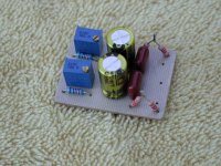
One thing was left out from my previous post and that is grounding schem, let see if I don't confuse you more.
Decided on a star ground located at the point of the DAC ground explained on my previous post, just bellow the current injection PCB. Since this point was somewhat inaccesible so most connection were made on the top of the small PCB over the same wire connecting this point.
So the +-8V power supply ground cable, which was tied at the output of the PSU board, is connected to this "star ground point"
Now, each channel on the OPA660 PCB has separate ground planes so from each channel there is a ground wire going to the "star ground point".
The output ground to the cinches (RCA's) was taken from each ground at the OPA PCB at the return point of each channel (screwed terminal post, the one at the center edge of the PCB.
I also decided not to run the ground of the I/V resistor through the ground plane (mostly power supply ground). So I have a separate wire running from the I/V resistor to a point near the ground return screw post from each channel on the OPA PCB.
Changing to the +-8V rails:
From the PSU there is one wire comming with the +8V and one with the -8V. Each one comes to one screwed post terminal and from there is distributed with wires to each 1000uf input cap (bypassed with 0.47uf film cap) before the LT431 shunt regulators. I did this for some obscure reason and not that I could not include these routings to the PCB.
Attachments

tony
hi,
why don't you try to skip the internal buffer in the opa660 - and use the buf634 instead, with separet vregs.....? i think it will be a great improvement......!

best regards,
troels
hi,
why don't you try to skip the internal buffer in the opa660 - and use the buf634 instead, with separet vregs.....? i think it will be a great improvement......!
best regards,
troels
Re: tony
That's something that could be tryed but really don't know if there will be improvement.
I guess this will work fine if the load to the output is high, say 10K or less?
The load at the line amp I'm using is 50K and the cable capacitance is only 50pf. Do you really think the sound can improve? and in what way?
Spec for the OPA660 are quite outstanding and it does not use feedback, IIRC aslo the Buf does not use FB.
Other opinions anyone?
tbla said:hi,
why don't you try to skip the internal buffer in the opa660 - and use the buf634 instead, with separet vregs.....? i think it will be a great improvement......!
That's something that could be tryed but really don't know if there will be improvement.
I guess this will work fine if the load to the output is high, say 10K or less?
The load at the line amp I'm using is 50K and the cable capacitance is only 50pf. Do you really think the sound can improve? and in what way?
Spec for the OPA660 are quite outstanding and it does not use feedback, IIRC aslo the Buf does not use FB.
Other opinions anyone?
apassgear said:Other opinions anyone?
Similarly to the input stage, the output buffer of the OPA660 is also diamond transistor, which means this buffer is the good one.
Pedja
tonitze said:Any other substitutes for opa660 since that it is not available either in RS or Farnel.
Sorry, I can't help with that information. The only supplier I know is DigiKey for the SOIC size over this part of the world.
Hope some other member can help.
P.S.
Certainly think there is no substitute for the OPA660.
Now that I have 25+ hours of break-in I can add some comments:
The old CDP (or not old any more?) is firmly sitting at the command post of my system delivering hi resolution audio waves and after this period has opened quite a bit.
This has lead to better high freq and low level resolution making the soundstage quite deep and wide with an integration to the sound that I have not experienced before.
I guess, besides the innerent qualities of the OPA, the way this circuit was implemented is responsible for an outstanding channel separation giving a solid image to instrument placing including those that are way to the left or right of the speakers.
All this is possible with the standard clock and PSU of the CDP, except of couse the one feeding the OPA.
So I expect further improvements when the clock and PSU are upgraded.
Still there is a lot of improvements to be had from the analog circuit since this implementation was done using few "audio" components. Case in point is the fact that all resistors used had steel caps (magnetic) and were carbon films. The one used at the I/V I had it mark as been a metalic film but I'm not sure about that.
The only parts used that could be said they are "audio" components are the decoupling caps of the OPA which are a 220u Panasonic FC 50V and the film caps that are polypropylene as was the 1n film cap used as filter in parallel to the I/V resistor (which I might get rid of it very soon).
I have change the output cap to a 5u6 (from 3u9) since with certain material (CD's) the bass was somewhat lacking. With the new cap all CD's sounds now convincing and did not found any degradation in sound.
Kuei,
How this stage would compare to I/V stage based on OPA 627?
I'm currently using OPA 627 and I'm wondering if it would be worthwile to change to OPA 660?
How this stage would compare to I/V stage based on OPA 627?
I'm currently using OPA 627 and I'm wondering if it would be worthwile to change to OPA 660?
Re: OPA660 I/V for TDA1545
Thank you, Kuei for the schematic - your output is prodigious- I have not checked in for a couple of days so only picked this up today - I will attempt to build this when I get some backup TDA1545 DACs as insurance.
Would piggybacking two DACs increase the output voltage or is this a no-no soundwise?
Thanks again
John
by Kuei Yang WangRe: OPA660 I/V for TDA1545
Thank you, Kuei for the schematic - your output is prodigious- I have not checked in for a couple of days so only picked this up today - I will attempt to build this when I get some backup TDA1545 DACs as insurance.
Would piggybacking two DACs increase the output voltage or is this a no-no soundwise?
Thanks again
John
Re: Re: OPA660 I/V for TDA1545
Konnichiwa,
The 1545 has a fixed, programmed in ratio between I bias and Iout. If I interpretetd the datasheet correctly you will see around 5V across the I/V resistor and in such a case the output will remain low. If the voltage is much lower than 5V then I have interpreted the Datasheet wrongly and bringing the DC voltage across the IV resistor to 5V (scale the value up) will raise the output.
Sayonara
Konnichiwa,
jkeny said:Would piggybacking two DACs increase the output voltage or is this a no-no soundwise?
The 1545 has a fixed, programmed in ratio between I bias and Iout. If I interpretetd the datasheet correctly you will see around 5V across the I/V resistor and in such a case the output will remain low. If the voltage is much lower than 5V then I have interpreted the Datasheet wrongly and bringing the DC voltage across the IV resistor to 5V (scale the value up) will raise the output.
Sayonara
Peter Daniel said:
How this stage would compare to I/V stage based on OPA 627?
I'm currently using OPA 627 and I'm wondering if it would be worthwile to change to OPA 660?
Would you mind telling us how did you connect the OPA627 as an I/V converter?
And what type of resistor did you use as I/V?
Would also like to know if you are using an output cap from the analog stage and if so which are you using?
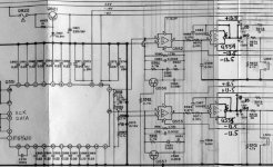
Here's the schematic of the output stage of my Marantz CD-94. I used only first ICs pair (Q552 and Q553). The signal from pin 6 and 25 of DACs output goes directly to the op amps (OPA627), I removed the resistors network used for DC cancelation. Everything in the op amps feedback circuit was replaced by one Vishay 1k resistor (the closest value I had) in parallel with 0.0022 Wima cap. I wanted to get away without using cap, but it sounded strange to my ears. Then from the IC's output signal goes directly to the players output through series 60 ohm Vishay resistor and 4.7 BG N coupling cap.
Attachments
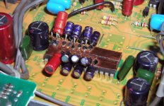
Here's how I did bypassing of all 14 pins of TDA1541. It doesn't get any smaller than that😉 I used 12 BG Hi Q 0.47 caps and two 4.7 caps on the other two pins. I can't comment on bass improvement as I'm listening through minimonitors at the moment, but low level high freq detail is better. Was it worth it? I'm not sure, ...probably😉
The copper foil strip on top of the DAC is both shielding for the chip and ground plain for the caps. I cut it later in half as I thought it might be better this way. Now I can also claim that I'm using double crown version😉
The copper foil strip on top of the DAC is both shielding for the chip and ground plain for the caps. I cut it later in half as I thought it might be better this way. Now I can also claim that I'm using double crown version😉
Attachments
Peter Daniel said:Here's how I did bypassing of all 14 pins of TDA1541. It doesn't get any smaller than that😉 I used 12 BG Hi Q 0.47 caps and two 4.7 caps on the other two pins. I can't comment on bass improvement as I'm listening through minimonitors at the moment, but low level high freq detail is better. Was it worth it? I'm not sure, ...probably😉
The copper foil strip on top of the DAC is both shielding for the chip and ground plain for the caps. I cut it later in half as I thought it might be better this way. Now I can also claim that I'm using double crown version😉
Very much liked the way you installed the 14 caps, it never occurred to me doing something like that.
Will do the same as soon as I can get some better caps.
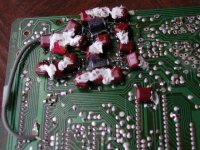
And this is the way I have it, underneath the board, very crowded with not enough vertical space.
Peter Daniel said:Here's how I did bypassing of all 14 pins of TDA1541. It doesn't get any smaller than that😉 I used 12 BG Hi Q 0.47 caps and two 4.7 caps on the other two pins. I can't comment on bass improvement as I'm listening through minimonitors at the moment, but low level high freq detail is better. Was it worth it? I'm not sure, ...probably😉
The copper foil strip on top of the DAC is both shielding for the chip and ground plain for the caps. I cut it later in half as I thought it might be better this way. Now I can also claim that I'm using double crown version😉
Very much liked the way you installed the 14 caps, it never occurred to me doing something like that.
Will do the same as soon as I can get some better caps.
And this is the way I have it, underneath the board, very crowded with not enough vertical space.
Attachments
Peter Daniel said:Here's the schematic of the output stage of my Marantz CD-94. I used only first ICs pair (Q552 and Q553). The signal from pin 6 and 25 of DACs output goes directly to the op amps (OPA627), I removed the resistors network used for DC cancelation. Everything in the op amps feedback circuit was replaced by one Vishay 1k resistor (the closest value I had) in parallel with 0.0022 Wima cap. I wanted to get away without using cap, but it sounded strange to my ears. Then from the IC's output signal goes directly to the players output through series 60 ohm Vishay resistor and 4.7 BG N coupling cap.
I get the picture on the I/V.
If you have not done it yet I would suggest removing all the circuit related to deemphasis. Q556/557 plus the two related caps and the two resistors from each channel since you still have a connection through the 4.7M resistor with possible leakege from the transistors and this may cause some smearing.
OPA660 I/V for TDA1545
Keui,
I have tried the single supply (10V) IV circuit for TDA1545 but can't seem to get it working.
DAC out and Vref pins are 3.33V but output from pin 8 on OPA660 accross 2K res is only 0.38V?
Any ideas?
Thanks John
Keui,
I have tried the single supply (10V) IV circuit for TDA1545 but can't seem to get it working.
DAC out and Vref pins are 3.33V but output from pin 8 on OPA660 accross 2K res is only 0.38V?
Any ideas?
Thanks John
Re: OPA660 I/V for TDA1545
Konnichiwa,
Is this at digital silence? Can you try a CD-Player with a CD with a -90.31dbfs 1KHz signal on it and check the DC as well as AC ('scope) on pin 8?
You could try increasing the 2K resistor, but even if I have the relationship between Bias and Output current wrong (polarity) you should get more voltage than 0.38V.
You can always connect a 1K resistor on the TDA1545 output and no OPA660 connected, this should give around 2.5V DC and 0.7V RMS signal (probabaly distorted/clipped).
If this is so, then connecting only the input section of the OPA660 (no buffer) is step two, which should yield 5V across the 2K resistor and 1.4 RMS Signal (definitly undistorted). Then you can connect the buffer.
Ciao T
Konnichiwa,
jkeny said:Keui,
I have tried the single supply (10V) IV circuit for TDA1545 but can't seem to get it working.
DAC out and Vref pins are 3.33V but output from pin 8 on OPA660 accross 2K res is only 0.38V?
Any ideas?
Is this at digital silence? Can you try a CD-Player with a CD with a -90.31dbfs 1KHz signal on it and check the DC as well as AC ('scope) on pin 8?
You could try increasing the 2K resistor, but even if I have the relationship between Bias and Output current wrong (polarity) you should get more voltage than 0.38V.
You can always connect a 1K resistor on the TDA1545 output and no OPA660 connected, this should give around 2.5V DC and 0.7V RMS signal (probabaly distorted/clipped).
If this is so, then connecting only the input section of the OPA660 (no buffer) is step two, which should yield 5V across the 2K resistor and 1.4 RMS Signal (definitly undistorted). Then you can connect the buffer.
Ciao T
- Status
- Not open for further replies.
- Home
- Source & Line
- Digital Source
- Opa660 I/V