Kuei Yang Wang said:
Well, the schematic was drawn by a friend and contains some errors. However, the Tilter pin's of the TDA1541 are all negative in Voltage (I measured), so the Cap needs to go positive to ground. I used 3u3 BTW.
Thanks for the confirmation, I will change the polarity of those caps.
🙂 🙂 🙂
Guido Tent said:
Maybe you mean:
" I'm delighted with my new CDP, so much that I do not need the improvement brought by updating the clock and adding a better supply to the DAC "
Appreciate you dropped in Guido.
As noted to Peter I have had second thoughts regarding my comment and will follow my first intention of redoing the clock and PSU.
I maybe want to do it myself (clock). Any suggestion on a system that works well on this environment?
I/V circuit setup
Hi Tony & Kuei,
ho to setup that 500R trimmer?
Where can I find the OPA660 in Italy or Europe?
Best regards.
Marco
Hi Tony & Kuei,
ho to setup that 500R trimmer?
Where can I find the OPA660 in Italy or Europe?
Best regards.
Marco
Re: I/V circuit setup
Marco,
I know that Digi Key stocks SOIC size in USA but could not tell who does in Europe. Maybe Kuei or other member can help with this.
Regarding the pot, is used to zero the buffer output so that AC is centered at zero volts reffered to ground.
This is done with no signal connecting your voltmeter to the point between the 47R and 3.9u output cap and the other lead to ground.
If your circuit is cold you need to set it at arround +25 mV since it will drift downhards when it warms. A presice value is not needed. I would say +-25 mV for the setting is OK.
mevangel said:Hi Tony & Kuei,
ho to setup that 500R trimmer?
Where can I find the OPA660 in Italy or Europe?
Best regards.
Marco,
I know that Digi Key stocks SOIC size in USA but could not tell who does in Europe. Maybe Kuei or other member can help with this.
Regarding the pot, is used to zero the buffer output so that AC is centered at zero volts reffered to ground.
This is done with no signal connecting your voltmeter to the point between the 47R and 3.9u output cap and the other lead to ground.
If your circuit is cold you need to set it at arround +25 mV since it will drift downhards when it warms. A presice value is not needed. I would say +-25 mV for the setting is OK.
It drifts.
Koinichiwa,
I suspect it drifts too much. But it should be possible to add a Servo with a mere +/-100mV "pull" range which should minimise it's sonic effect. Except it replaces a large value capacitor for coupling with a small value cpacitor plus a bunch or resistors and an Op-Amp and it often sounds worse, so I personally would not bother.
Sayonara
Peter Daniel said:So it might be possible to use the circuit without coupling cap. Or does it drift too much?
I suspect it drifts too much. But it should be possible to add a Servo with a mere +/-100mV "pull" range which should minimise it's sonic effect. Except it replaces a large value capacitor for coupling with a small value cpacitor plus a bunch or resistors and an Op-Amp and it often sounds worse, so I personally would not bother.
Sayonara
Kuei Yang Wang said:Koinichiwa,
I suspect it drifts too much. But it should be possible to add a Servo with a mere +/-100mV "pull" range which should minimise it's sonic effect. Except it replaces a large value capacitor for coupling with a small value cpacitor plus a bunch or resistors and an Op-Amp and it often sounds worse, so I personally would not bother.
Sayonara
Hi
Servo's may interact quite surprisingly, I recall a piece of software on the net that lets you calculate the right servo components. Will try to dig it up
best regards
Guido Tent said:
Hi
Servo's may interact quite surprisingly, I recall a piece of software on the net that lets you calculate the right servo components. Will try to dig it up
best regards
got it !
http://www.danbbs.dk/~ko/dcservo.htm
nice music at the background as well (actually Donald Fagen was my first vinyl record I bought)
enjoy
OPA660 I/V for TDA1545
Can someone detail how schematic can be modified for use with TDA1545?
Thanks
Can someone detail how schematic can be modified for use with TDA1545?
Thanks
Peter Daniel said:So it might be possible to use the circuit without coupling cap. Or does it drift too much?
As suspected it does drift, arround 25mV but haven't obseved how stable it is when warm since anyway it needs the coupling cap.
And also think a coupling cap is better than a servo plus having the assurance that you won't have any DC at the output.
Re: OPA660 I/V for TDA1545
Can't find the data sheet for the TDA1545 on the net. I wanted this to check the current output spec of the DAC. This is needed to adjust the values of the current injection portion of the circuit.
This current injection part of the circuit is shown on the left lower corner of the schematic, connected to the DAC output.
In the case of the schematic shown is set to inject +2mA to this point, 5V/2500 Ohms= 2mA. Before you ask, yes, the total resistor values does not add up to 2.5K I had to adjust them in order to be able to zero the Buffer. This might be due to the DAC that may not be exact to spec.
The other element that has to be checked is the I/V resistor which also need to be compliant with the DAC output caracteristics.
All other parts of the circuit are not related to the DAC so they can be left as is.
I'll try to dig some information on this DAC and let you know If I find something.
jkeny said:Can someone detail how schematic can be modified for use with TDA1545?
Thanks
Can't find the data sheet for the TDA1545 on the net. I wanted this to check the current output spec of the DAC. This is needed to adjust the values of the current injection portion of the circuit.
This current injection part of the circuit is shown on the left lower corner of the schematic, connected to the DAC output.
In the case of the schematic shown is set to inject +2mA to this point, 5V/2500 Ohms= 2mA. Before you ask, yes, the total resistor values does not add up to 2.5K I had to adjust them in order to be able to zero the Buffer. This might be due to the DAC that may not be exact to spec.
The other element that has to be checked is the I/V resistor which also need to be compliant with the DAC output caracteristics.
All other parts of the circuit are not related to the DAC so they can be left as is.
I'll try to dig some information on this DAC and let you know If I find something.
Re: OPA660 I/V for TDA1545
Koinichiwa,
The TDA1545 will have 2.5 - 3V DC offset on the output. Hence the circuit changes are not straightforward. I'll look at it when I can, as a few "fancy" things are needed to make that wirk without adding caps etc....
Sayonara
Koinichiwa,
jkeny said:Can someone detail how schematic can be modified for use with TDA1545?
The TDA1545 will have 2.5 - 3V DC offset on the output. Hence the circuit changes are not straightforward. I'll look at it when I can, as a few "fancy" things are needed to make that wirk without adding caps etc....
Sayonara
OPA660 i/v for TDA1545
Thanks Keui, Tony,
Datasheet at http://www.semiconductors.philips.com/acrobat/datasheets/TDA1545A_T_3.pdf
As Keui says TDA1545 wil have about 3.3V on Vref (which has to be catered for) and therefore some dc on output.
Look forward to any/all suggestions
John
Thanks Keui, Tony,
Datasheet at http://www.semiconductors.philips.com/acrobat/datasheets/TDA1545A_T_3.pdf
As Keui says TDA1545 wil have about 3.3V on Vref (which has to be catered for) and therefore some dc on output.
Look forward to any/all suggestions
John
Re: OPA660 i/v for TDA1545
Koinichiwa,
There are two ways I can think of now.
Use a seperate supply for the Analogue stage with the ground lifted to "Vref".
Or use a single +10V supply which would however require a DC blocking capacitor on the I/V resistor or some form of offset correctionwith resistors to ground and to +10V and the output shifted to +5V and AC coupled to the outside world. I need to think about that. Maybe the Bias current from the DAC could be used to shift the output from the current conveyer just right, I need to play with the idea...
Sayonara
Koinichiwa,
jkeny said:As Keui says TDA1545 wil have about 3.3V on Vref (which has to be catered for) and therefore some dc on output.
Look forward to any/all suggestions
There are two ways I can think of now.
Use a seperate supply for the Analogue stage with the ground lifted to "Vref".
Or use a single +10V supply which would however require a DC blocking capacitor on the I/V resistor or some form of offset correctionwith resistors to ground and to +10V and the output shifted to +5V and AC coupled to the outside world. I need to think about that. Maybe the Bias current from the DAC could be used to shift the output from the current conveyer just right, I need to play with the idea...
Sayonara
OPA660 i/v for TDA1545
Thanks Kuei,
Slightly off topic - does anyone know of source for TDA1545 DAC - I have one from CD4000 CDP which I intend to use but want to build a buffer against mishaps.
Thanks
Thanks Kuei,
Slightly off topic - does anyone know of source for TDA1545 DAC - I have one from CD4000 CDP which I intend to use but want to build a buffer against mishaps.
Thanks
Re: OPA660 I/V for TDA1545
Koinichiwa,
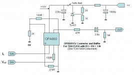
I had a bash. Note, the suggested Schematic is neither tested or simulated and that I may have gotten my reading of the datasheets wrong. So, it SHOULD work, but no garantes...
Anyway, this requires the TDA1545 to operate at the top of the specified output current and still only gives 4V peak-Peak (1.414V RMS) output for full scale, so the output will be 3db quieter than "standard", sorry can't do it any other way without .
Anyway, the circuit is simple enough.
The OPA660 will draw around 20-26mA current. If we run the TL431 at the same current for a nominal +12V supply voltage (12V SLA Battery) the series resistor in the PSU should be 39R. I think an active CCS with low dropout (LM1085?) is preferable....
The base input of the "current conveyor" is being set to 3.33V and thus the DAC output is being held at 3.33V also. The DAC has a bias current of around 1.5mA and an output current of 1mA for digital silence which can deviate by +/-1mA.
So at digital silence the current into the I/V conversion resistor of 2k will be 2.5mA giving us 5V across it, neatly biasing the output of the "current conveyor" and the input of the buffer to 1/2 V+. The powersupply is single rail only of course, the output is at +5V.
With +/-1mA variation in current for a full scale sinewave we get +/-2V or 1.414V RMS output Voltage. That's it.
If you like add a Capacitor in parallel with the I/V resistor for a lowpass, you could build a 2nd or 3rd order Sallen Key LPF around the Buffer, including a peaking one allowing "anti sinc" correction for non-oversampling DAC's, you have many options to refine this basic scheme....
Sayonara
Koinichiwa,
jkeny said:Can someone detail how schematic can be modified for use with TDA1545?
I had a bash. Note, the suggested Schematic is neither tested or simulated and that I may have gotten my reading of the datasheets wrong. So, it SHOULD work, but no garantes...
Anyway, this requires the TDA1545 to operate at the top of the specified output current and still only gives 4V peak-Peak (1.414V RMS) output for full scale, so the output will be 3db quieter than "standard", sorry can't do it any other way without .
Anyway, the circuit is simple enough.
The OPA660 will draw around 20-26mA current. If we run the TL431 at the same current for a nominal +12V supply voltage (12V SLA Battery) the series resistor in the PSU should be 39R. I think an active CCS with low dropout (LM1085?) is preferable....
The base input of the "current conveyor" is being set to 3.33V and thus the DAC output is being held at 3.33V also. The DAC has a bias current of around 1.5mA and an output current of 1mA for digital silence which can deviate by +/-1mA.
So at digital silence the current into the I/V conversion resistor of 2k will be 2.5mA giving us 5V across it, neatly biasing the output of the "current conveyor" and the input of the buffer to 1/2 V+. The powersupply is single rail only of course, the output is at +5V.
With +/-1mA variation in current for a full scale sinewave we get +/-2V or 1.414V RMS output Voltage. That's it.
If you like add a Capacitor in parallel with the I/V resistor for a lowpass, you could build a 2nd or 3rd order Sallen Key LPF around the Buffer, including a peaking one allowing "anti sinc" correction for non-oversampling DAC's, you have many options to refine this basic scheme....
Sayonara
Attachments
I will try to address several questions of general interest that have been ask by private mail and also try overcome some answers I have been short in replays such as the one to Peter Daniel regarding PSU.
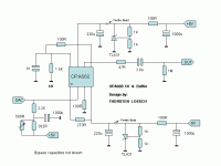
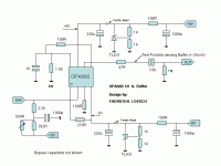
First of all let me say that I tryied to follow all recomendations suggested by Thorten Loesch (Kuei Yang Wang) and that the original posted schematic by me (post #46, one channel shown) is intended for use with TDA1541A DAC.
The OPA660 is a special kind of chip since is not a regular Op Amp and comprises two sections (please see Data Sheet). The fist section where the I/V takes place it's called Operational Transconductance Amplifier (OTA) where you can see a 1.5K resistor coming from pin 8 to ground, that's the I/V resistor which is paralleled with a 1n cap. The cap is a first order filter for unwanted high freq. reflexions. this cap can be omited or increases up to 2n4 in case you think you need a lower low pass filter. Depending on your amplifiers and using oversampling you may well do without any filtering.
When you use non-oversampling circuit you may want a second order filter, once again, depending on amplification and taste. In this case you can go with a 1nf cap in parallel with the I/V resistor and a 33nf at the output of the OPA Buffer (I guess the correct position would be from the "test point" (on the schematic) to ground.
Now, the second section of the OPA660 is a buffer which is connected from pin 8 to pin 5 (the input of the buffer) with a 100 Ohms resistor. The output of the buffer is pin 6.
Most of the following is the way I implemented the circuit so feel free to experiment simpler or more elaborated approaches:
The circuit was built using two PCB. The first one a very small one is used for the current injection, the circuit for this part of the implementation is the one shown in the lower left corner of the schematic which needs a +5V supply. If you look to post #1 you will see in the picture a small PCB sitting in front of the DAC on the main board, that's the one.
This current injection is needed one for each channel but I used only one +5V supply for both channels. The way this is built forms a filter to the +2 mA comming from the single +5V supply so little crosstalk will be had from channel to channel.
Since the outputs from the DAC had two jumpers (one for each channel) going to the analog stages I lifted these from the far side and made there the connection to the current injection board. The ground needed for this circuit was taken from the point where the DAC takes ground from the top ground plane on the main board. This ground is taken to the DAC through a jumper which is soldered to this ground plane just bellow the small PCB. Hope I don't confuse you.
The second board shown on the upper right side of the pic on post #1 contains the rest of the circuit shown on the schematic (including the OPA660 on the copper side) with exception of the 3u9 output cap and 1M resistors that are attached to the cinch RCA output female connectors.
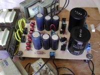
PSU:
Both +-8V supplys, only one each, were built on a separate "chassis" using one 12v secondary transformer and 4 fast recovery diodes (full wave bridge) for each rail. These diodes were bypassed with 0.47u 50V film caps. The bridges feed the first 4700u 35V caps connecting through a 10 Ohms 1W resistors(both positive and ground or negative and ground) so 2 resistors per rail to 2x 2,200uf 25V per rail. Next comes the preregs using LM417T and LM437T which are bypassed at the adjust pin with 10uf lytic plus 0.47uf film cap (see data sheet for more info). From the regs they go to a last set of 4700uf lytic caps. At this point I'm bleeding some 11mA current through a 750 Ohms resistors at each rail. See pic...
The +5V for the current injection was taken from the main board PSU at a point just before entering the 10 Ohms input resistor suppling the DAC. I may change this in the future since I intend to make separate supply for the DAC.
P.S.
Please also note that schematic at post #46 does not show bypass capacitors needed at the power supply to the OPA660.
First of all let me say that I tryied to follow all recomendations suggested by Thorten Loesch (Kuei Yang Wang) and that the original posted schematic by me (post #46, one channel shown) is intended for use with TDA1541A DAC.
The OPA660 is a special kind of chip since is not a regular Op Amp and comprises two sections (please see Data Sheet). The fist section where the I/V takes place it's called Operational Transconductance Amplifier (OTA) where you can see a 1.5K resistor coming from pin 8 to ground, that's the I/V resistor which is paralleled with a 1n cap. The cap is a first order filter for unwanted high freq. reflexions. this cap can be omited or increases up to 2n4 in case you think you need a lower low pass filter. Depending on your amplifiers and using oversampling you may well do without any filtering.
When you use non-oversampling circuit you may want a second order filter, once again, depending on amplification and taste. In this case you can go with a 1nf cap in parallel with the I/V resistor and a 33nf at the output of the OPA Buffer (I guess the correct position would be from the "test point" (on the schematic) to ground.
Now, the second section of the OPA660 is a buffer which is connected from pin 8 to pin 5 (the input of the buffer) with a 100 Ohms resistor. The output of the buffer is pin 6.
Most of the following is the way I implemented the circuit so feel free to experiment simpler or more elaborated approaches:
The circuit was built using two PCB. The first one a very small one is used for the current injection, the circuit for this part of the implementation is the one shown in the lower left corner of the schematic which needs a +5V supply. If you look to post #1 you will see in the picture a small PCB sitting in front of the DAC on the main board, that's the one.
This current injection is needed one for each channel but I used only one +5V supply for both channels. The way this is built forms a filter to the +2 mA comming from the single +5V supply so little crosstalk will be had from channel to channel.
Since the outputs from the DAC had two jumpers (one for each channel) going to the analog stages I lifted these from the far side and made there the connection to the current injection board. The ground needed for this circuit was taken from the point where the DAC takes ground from the top ground plane on the main board. This ground is taken to the DAC through a jumper which is soldered to this ground plane just bellow the small PCB. Hope I don't confuse you.
The second board shown on the upper right side of the pic on post #1 contains the rest of the circuit shown on the schematic (including the OPA660 on the copper side) with exception of the 3u9 output cap and 1M resistors that are attached to the cinch RCA output female connectors.
PSU:
Both +-8V supplys, only one each, were built on a separate "chassis" using one 12v secondary transformer and 4 fast recovery diodes (full wave bridge) for each rail. These diodes were bypassed with 0.47u 50V film caps. The bridges feed the first 4700u 35V caps connecting through a 10 Ohms 1W resistors(both positive and ground or negative and ground) so 2 resistors per rail to 2x 2,200uf 25V per rail. Next comes the preregs using LM417T and LM437T which are bypassed at the adjust pin with 10uf lytic plus 0.47uf film cap (see data sheet for more info). From the regs they go to a last set of 4700uf lytic caps. At this point I'm bleeding some 11mA current through a 750 Ohms resistors at each rail. See pic...
The +5V for the current injection was taken from the main board PSU at a point just before entering the 10 Ohms input resistor suppling the DAC. I may change this in the future since I intend to make separate supply for the DAC.
P.S.
Please also note that schematic at post #46 does not show bypass capacitors needed at the power supply to the OPA660.
Attachments
- Status
- Not open for further replies.
- Home
- Source & Line
- Digital Source
- Opa660 I/V