The PCB is designed for BS170 (DGS):I have the rev D pcb and refered to the shematic from post #42 where Q51/53 are BS170 (DGS) types.
In Omicron protection explanation from post #34 2N7002 (SGD) were used.
I´ve used BS170. That might be the issue...
By itself, it is not a problem, but I would be curious why the two channels differ that much.The bias differs arround 5mA from left to right channel. Is this tolerable or do I need to readjust?
Those are excellent transistors and should work well. Since they are much faster compared to BD19/BD140, it might make sense to check the output (pre-inductor) for oscillations - if you have a scope. Emitter followers can be tricky sometimes.And I´ve used 2SC3421/2SA1358 instead BD139/140.
Did not test with +/-12V but would expect no problem.Will +/-12V supply are also sufficient? That will lower the heat.
Nice work Alex! I love some simple circuits and you achieved this with relatively few part count. Congrats!

The distortion is so low I can’t tell if it’s third order or second order dominant at higher drive levels?
Would using OPA1656 instead of NE5532 change things for the better?
Is this still the current schematic for basic amp?

The distortion is so low I can’t tell if it’s third order or second order dominant at higher drive levels?
Would using OPA1656 instead of NE5532 change things for the better?
Is this still the current schematic for basic amp?


Thank you!Nice work Alex! Congrats!
Honestly, at Omicron's distortion level, I am now sure if that's a meaningful question. Typically, the prevalence of second or third order distortion affects the way an amplifier sounds, with different listeners having different preferences. However, with the distortion as low as it is in Omicron, you don't hear that distortion anymore. It is an interesting auditory experience when your amplifier adds neither dirt no fairy dust.The distortion is so low I can’t tell if it’s third order or second order dominant at higher drive levels?
Nope, OPA1656 is a fine opamp but too fast (has too large GBW) for the frequency compensation shown in the schematic, so it is likely to oscillate. NE5532 is recommended, other opamps with GBW in the range of 8..16MHz can be tested. TL072 gives good results although, understandably, it is not as linear as NE5532 (see also post #42).Would using OPA1656 instead of NE5532 change things for the better?
Yes, although the SMT version will use different parts.Is this still the current schematic for basic amp?
Last edited:
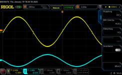
That's not even close to what is should look like - the actual clip is shown in post #11.Some screenshots with sine 1kHz in 16R resistor load, right channel:
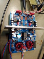
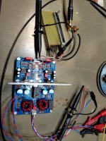
Let's dig in to figure it out. First, post here a photo of your assembled board.
Second, your clipping is asymmetric and at only +4 volts - it should be perfectly symmetric and just a couple of volts below your power supply rails (Omicron clips at +/-15V with +/-17V power supply). The prime suspect are the biasing and bias currents. Make sure that C9 and C10 have correct values and are soldered in with the correct polarity. Measure the emitter resistors R15/R16 with the power off to verify they are 2.2 ohm, then measure voltage drop across each of them with power on but without any input signal. Post the results here.
Based on that, we will take it forward.
Last edited:
Good question - I am curious, too. With asymmetric clipping at just 4 volts and the DC protection triggered, something is amiss in that particular build. We'll figure it out.What’s going on at the zero crossing?
Last edited:
Nice build! I like your socketing the crossfeed! 👍
Let's fix that and see where it takes us.Looks like the emitter resistors are the bad.
Back again with new porn 😉
When I push the input volume a bit more DC protection jumps in.
Known hardware bugs fixed. Bias is set to aprox 100mA per channel.
Voltage drop accross R15/16 98mV respectively R35/36 95mV.
I listened to some music with in ears 30Ohms and the big cans 16Ohms.
Max volume with the big ones is too low, bass deep and well pronounced, voices a bit muddy.
The in ears produced a totaly different sound, bass and treble extremely sharp and metalic, voices very far away and extrem low volume with an echo...
Hard to describe...
With my Whammy the two headphones are not to far from another.
That´s a strange experience
Last edited:
Let us unpack this a bit.
First, your initial problem was that the DC protection did not connect the load. What was the problem, and what did you do to fix that?
Second, did you check your output transistors after replacing the emitter resistors? Depending on your power supply, running them with zero ohm emitter resistors might have undesired consequences.
Third, a voltage drop of 98mV across 2.2 ohm (R15 or R16 or R35 or R36) corresponds to about 45mA, not 100mA. What is the actual bias current in each channel? Is it identical in the positive and negative half of each channel's output stage? (What is the voltage drop across each of R15, R16, R35 and R36)? What is the DC voltage at the output of each channel without any input signal?
Fourth, the scope pictures need some explanation. What is each trace in each picture? It that one channel or both? Under what conditions these were taken (supply voltages, bias currents, load)? In particular, what's the difference between pictures showing clip at 4V peak and those clipping at 10V peak? What is the difference between pictures showing artifacts at zero crossing and others that don't?
Fifth, all clipping appears to be at the positive half only. How does the amp clip at the negative side?
Finally, I would not listen to any amp in this condition. Something is wrong, and you won't get the intended performance until you find and fix the problem(s).
I changed the 2N700 to BS170 and 2N3906 to BC327 (I had no more 2N3906). The relais/DC protection is working fine now.First, your initial problem was that the DC protection did not connect the load. What was the problem, and what did you do to fix that?
The current limit of my power supply is set to 500mA. This should not be a danger for the 2SC3421/2SA1358 (Ic=1A).Second, did you check your output transistors after replacing the emitter resistors? Depending on your power supply, running them with zero ohm emitter resistors might have undesired consequences.
You´re absolutely right. I have confused this with the current display from the power supply unit which is +113/-115mA for both channels together 🙄Third, a voltage drop of 98mV across 2.2 ohm (R15 or R16 or R35 or R36) corresponds to about 45mA, not 100mA. What is the actual bias current in each channel? Is it identical in the positive and negative half of each channel's output stage? (What is the voltage drop across each of R15, R16, R35 and R36)? What is the DC voltage at the output of each channel without any input signal?
That does irritate me. I have increased R13/14 and R33/34 from 47R to 120R. This gives the current Ibias=45mA. Before that was only about half. Maybe the output transistors have a different hfe from BD139/140...
The bias current is nearly identical (difference 1mA) in both channels and on both rails.
DC voltage at output is 2mV left and 1mV right channel.
Sorry, you can't see the names of the screenshots....Fourth, the scope pictures need some explanation. What is each trace in each picture? It that one channel or both? Under what conditions these were taken (supply voltages, bias currents, load)? In particular, what's the difference between pictures showing clip at 4V peak and those clipping at 10V peak? What is the difference between pictures showing artifacts at zero crossing and others that don't?
Yellow traces are left channel output.
Blue traces are right channel output.
Both with 16R resistor load, +/-15V supply, 45mA bias.
The artifacts are depending on the input level which I increased more and more. It begins with distortions at zero crossing.
I can´t force clipping on the negative side. This may be due to the maximum level of my generator, it´s 6Vpp?
Anyway DC protection jumps in before reaching 6Vpp
Last edited:
Thank you!
Looks like DC protection kicks in because of asymmetric clipping - when that happens, the output signal is no longer centered around zero, and the protection senses that.Anyway DC protection jumps in before reaching 6Vpp
That's good news. What is the DC voltage at the output of the second opamps - that is, at the point where R13 R14 C9 C10 (R33 R34 C29 C30 for the other channel) and the opamp's output connect?DC voltage at output is 2mV left and 1mV right channel.
Ok. How does the amp clip with a lighter load, e.g. 100 ohm? And when it clips, how does the signal look at the at the outputs of the second opamps?U1/P7=72mV
U21/P1=63mV
Good. The amp has no problem swinging its output but somehow fails to supply enough current to the load when the signal goes positive.
With the load connected, when the amp is clipping, what is the waveforms at the at the outputs of the second opamps?
With the load connected, when the amp is clipping, what is the waveforms at the at the outputs of the second opamps?
Now we are getting somewhere. The prime suspects are your NPN transistors - sorry. Let me explain.
First, a quick reminder that Omicron was designed to deliver 100mW RMS (200mW peak) into loads with the impedance of 32 to 600 ohms.
This is how Omicron clips into 30 ohm. Shown is a single channel, +/-17V power supply, 28mA quiescent current. The yellow trace is the channel's output, pink - the output of the second opamp (U1/P7). To put things into perspective, Omicron here delivers about 4 Watts, or 40 times the max power it was designed for:

This is the same channel clipping into 15ohms. Traces and conditions are the same as above. The output power now is about 5 Watts:

This:

and the lower amplitude at the output are signs of insufficient bias when delivering such a high power into an extremely low impedance load.
If you compare my second image above with what you observed

it becomes clear that the PNP parts of both your channels works exactly as it should, but the NPN part severely lacks bias under load.
Since you made sure that (1) the quiescent bias current is the same for both PNP and NPN transistors, (2) the quiescent voltage at the input of the emitter follower is not far from zero, and (3) the amplifier works just fine without a load, I conclude that the NPN transistors under load draw a much higher base current than expected.
Since both channels behave identically, as error in wiring the bias circuit (R11 R13 D7 C9) is not likely. What is likely is a problem with two transistors coming from the same bag. Mouser tells me the 2SC3421 is obsolete - are yours genuine?
I suggest you replace the transistors in one channel (not both) with the BD139/BD140 (preferably BD139-16 and BD140-16 if you can choose - these have a higher current gain) and see what that brings you. While you're at that, you should also ground the heatsink - the intended heatsinks are grounded through their pins, but your construction is different.
First, a quick reminder that Omicron was designed to deliver 100mW RMS (200mW peak) into loads with the impedance of 32 to 600 ohms.
This is how Omicron clips into 30 ohm. Shown is a single channel, +/-17V power supply, 28mA quiescent current. The yellow trace is the channel's output, pink - the output of the second opamp (U1/P7). To put things into perspective, Omicron here delivers about 4 Watts, or 40 times the max power it was designed for:
This is the same channel clipping into 15ohms. Traces and conditions are the same as above. The output power now is about 5 Watts:
This:
and the lower amplitude at the output are signs of insufficient bias when delivering such a high power into an extremely low impedance load.
With the peak output voltage at about 12V, the peak output current into 15 ohm is 0.8A. Assuming that the current gain of the output transistor is 60 (see the datasheet for the BD139), its peak base current would need to be 13mA. All of it is provided by C9/C10, and the current via R11/R12 is not enough to recharge the capacitors. As a result, when delivering 50 times the max power the amp was designed for, the bias collapses.
Under normal conditions, the peak output power of 200mW into 32 ohm corresponds to peak output voltage of 2.5V and peak output current of 80 mA. At that collector current, the current gain of the transistors is about 100, and the necessary base current is comfortably delivered by R11/R12 while C9/C10 maintain bias stability.
Under normal conditions, the peak output power of 200mW into 32 ohm corresponds to peak output voltage of 2.5V and peak output current of 80 mA. At that collector current, the current gain of the transistors is about 100, and the necessary base current is comfortably delivered by R11/R12 while C9/C10 maintain bias stability.
If you compare my second image above with what you observed
it becomes clear that the PNP parts of both your channels works exactly as it should, but the NPN part severely lacks bias under load.
Since you made sure that (1) the quiescent bias current is the same for both PNP and NPN transistors, (2) the quiescent voltage at the input of the emitter follower is not far from zero, and (3) the amplifier works just fine without a load, I conclude that the NPN transistors under load draw a much higher base current than expected.
Since both channels behave identically, as error in wiring the bias circuit (R11 R13 D7 C9) is not likely. What is likely is a problem with two transistors coming from the same bag. Mouser tells me the 2SC3421 is obsolete - are yours genuine?
I suggest you replace the transistors in one channel (not both) with the BD139/BD140 (preferably BD139-16 and BD140-16 if you can choose - these have a higher current gain) and see what that brings you. While you're at that, you should also ground the heatsink - the intended heatsinks are grounded through their pins, but your construction is different.
- Home
- Amplifiers
- Headphone Systems
- Omicron, a compact headphone amp with -140dB distortion