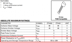
For better performance with lower impedance loads, versatility (common small BJTs such as 2N3904/3906 or BC546/556 can be used) and because there was enough space on the board after the heatsinks were removed. With beefier TO-92s such as PN2222/2907 or BC639/640, two pairs may be enough.

This reminds me of an amp that I used to carry around when Headwize was still up an running


not to derail your excellent work, rather a walk down memory lane 🙂 - this one uses a simple diamond buffer on the output
not to derail your excellent work, rather a walk down memory lane 🙂 - this one uses a simple diamond buffer on the output
Oh boy. I don't quite understand the infatuation with the diamond buffer, but I can assure you that a diamond buffer inside a single opamp's feedback loop doesn't have a chance to even come close to Omicron in linearity. We tested it and found it provides no benefit vs a simple push-pull emitter follower, while adding complexity and the cost of additional parts. Also, a diamond buffer with resistors in the emitters of the first stage and a single pair of BC550/560 in the second is not what I would want for my 32 ohm Grados.
One can add heatsinks to PN2222/2907, which are good for 1.5W. Still, multiple TO-92s or one pair in TO-126 on a heatsink is a more robust solution.Or use Zetex / Diodes Inc "Super E-Line" parts which are rated for 1.0 watts.
Last edited:
Yep, as I said. Memory lane. A decade ago and expanding beyond the cmoy tin amps of the time. I have moved beyond the Grado and opamps of yore. Enjoy the omicron and the excitement of development.
Hello Alex, hope you dont mind but i threw together a quick omicron (with crossfeed but no zobel) for personal use / testing.
Implemented on 4 layer pcb. For heatsink, from sims it only shows 130mW-ish, i'll bolt both output transistors together on the same heatsink. Hopefully they dont capacitatively couple something to each other due to the proximity, i dont know if im exxagerating it in my head though.
I also added feedback triming with pot (since sometimes i'd just like more gain / no need for so much nfb, or just to experiment around with), but im not sure if the critical feedback path having a pot in it would be a bad idea yet, guess we'll see.
Looks cool. I presume most capacitors are on the bottom?
I have a few comments:
First, if you change the gain in Omicron, you must adjust its frequency compensation. If you don't know how, just leave the gain alone.
Second, you need to take feedback from where your load is connected on the PCB - see, for example, this example from Douglas Self's book on power amplifiers:

Otherwise, the seemingly insignificant piece of trace between R35 and R36 will generate audible and measurable distortion.
Third, routing the so-called "ground" is critical for distortion performance. It is not clear from the 3D rendering how you did it, but If you have one "ground" layer where everything is connected, you are likely to have audible and measurable distortion a couple of orders of magnitude above what Omicron is capable of.
Overall, routing a PCB for an amp - any amp - in a way that keeps distortion low is not trivial, and the results can be disappointing. You've been warned 😉
I have a few comments:
First, if you change the gain in Omicron, you must adjust its frequency compensation. If you don't know how, just leave the gain alone.
Second, you need to take feedback from where your load is connected on the PCB - see, for example, this example from Douglas Self's book on power amplifiers:
Otherwise, the seemingly insignificant piece of trace between R35 and R36 will generate audible and measurable distortion.
Third, routing the so-called "ground" is critical for distortion performance. It is not clear from the 3D rendering how you did it, but If you have one "ground" layer where everything is connected, you are likely to have audible and measurable distortion a couple of orders of magnitude above what Omicron is capable of.
Overall, routing a PCB for an amp - any amp - in a way that keeps distortion low is not trivial, and the results can be disappointing. You've been warned 😉
Alex, how's the polishing going?Still polishing the SMT board...
Yeah, i put them as close as possible to minimise their trace lengthLooks cool. I presume most capacitors are on the bottom?
Hmm you're right. I remember playing around with My_ref in TI's TINA spice, it had a similar kind of global feedback loop, phase margin was very sensitive to the compensation cap, guess i got a bit ahead of myself here.I have a few comments:
First, if you change the gain in Omicron, you must adjust its frequency compensation. If you don't know how, just leave the gain alone.
Hmm...i see, thinking about what you said i see i could totally rework it then. I'll try to have the R35 and R36 as close to each other, and as close to the output pin, and do the same to the loop from the output to the inverting input of U1A (and minimise the whole length of).Second, you need to take feedback from where your load is connected on the PCB - see, for example, this example from Douglas Self's book on power amplifiers:
View attachment 1145225
Otherwise, the seemingly insignificant piece of trace between R35 and R36 will generate audible and measurable distortion.
But i still wonder, the load is the headphone transducer right? But that will always be on a 2 meter cable somewhere far away, so we only reduced the whole thing by a centimeter or two, just getting it a bit closer to the "output pin" on the PCB and from there on Jesus take the wheel. Am i misconstruing something? Isnt it kind of like using expensive mains cable for the final 2 meters of the electrical path inside your home, after the power already traveled through 2 kilometers of the city's cheap aluminium power lines, home depot cabling inside your walls, etc.
For ground i use copper pours yeah, but trying to be mindful of current return paths, by trying to have a sensible layout of components, not having lines cross over each other and share grounds excessively, it's true that i wouldn't be able to do this with 2 layers.Third, routing the so-called "ground" is critical for distortion performance. It is not clear from the 3D rendering how you did it, but If you have one "ground" layer where everything is connected, you are likely to have audible and measurable distortion a couple of orders of magnitude above what Omicron is capable of.
Thank you for your detailed reply 🙂Overall, routing a PCB for an amp - any amp - in a way that keeps distortion low is not trivial, and the results can be disappointing. You've been warned 😉
I have been warned indeed, we already know what omicron can do from official numbers so anything less than that is entirely my fault.
There's one thing i wanted to ask you that i was wondering about, why do we have so much resistors on non inverting side of first opamp stage, couldn't they all be reduced to one value (in this case 2k || 5k || 8.2k =~ 1.2k)? And when i tried it in the sim, connecting it straight to GND gave similar performance, does doing it this way improve phase margin or something?
Btw, for the zobel inductor, i dont know if you use Kicad or something else, but there's a plugin which "bakes in" the inductor as a trace on the pcb. It takes up some horizontal real estate, i guess its mostly used for some RF applications. Of course the benefits are that its perfectly repeatable, saves time on winding, and you get it "for free". Just saying if you want to check it out could be a useful thing in your arsenal.
Almost there 😉Alex, how's the polishing going?
I meant the point where the load is connected. Consider the long cord part of the load.the load is the headphone transducer right?
Three reasons:why do we have so much resistors on non inverting side of first opamp stage
- Equalize the impedances seen by each input
- Connect the non-inverting input to the right signal
- Minimize the area enclosed on the PCB by each signal of importance
I redid the layout keeping in mind some of your pointers, now i almost even (other than 1 trace) managed to route everything on just 2 layers, though i am still using a 4 layer board just so each trace can have an uninterrupted current return path beneath that does not cross (or minimally) other traces (the higher the frequency, the more closely it wants to follow the trace above, i.e minimum impedance path). The feeback loops, both the global and local, and the bjt degeneration resistors, are as close to the output as i could get them.
It looks a fit funny especially with the random mounting holes...but whatever, its just for personal use. Maybe you'll say it sux but anyway, thanks for the help and openess with this.


It looks a fit funny especially with the random mounting holes...but whatever, its just for personal use. Maybe you'll say it sux but anyway, thanks for the help and openess with this.
All the same comments apply, plus now the electrolytics in power supply rails are gone - not a good idea.
Say you have a trace connecting the two emitter resistors, with the output connected on one end, and feedback taken from the other:

Let's assume this trace is 0.1in long an 50mils wide, with 1oz copper, so that its resistance is around 1mOhm. If your load is 32 ohm, then the load will see 1m/32 = 0.003% of distortion right there, even if the rest of the amplifier does not distort at all. Bye-bye undistorted sound...
As I said above, I am happy to see you trying your hand at the board, but I cannot provide support for circuit modifications or custom PCBs, nor can I let anyone have the impression that I approve of any board other than our own - I do not. You are on your own there.
Say you have a trace connecting the two emitter resistors, with the output connected on one end, and feedback taken from the other:
Let's assume this trace is 0.1in long an 50mils wide, with 1oz copper, so that its resistance is around 1mOhm. If your load is 32 ohm, then the load will see 1m/32 = 0.003% of distortion right there, even if the rest of the amplifier does not distort at all. Bye-bye undistorted sound...
As I said above, I am happy to see you trying your hand at the board, but I cannot provide support for circuit modifications or custom PCBs, nor can I let anyone have the impression that I approve of any board other than our own - I do not. You are on your own there.
My very sketchy opinion: The layout and routing are a work of art. But, considering the goal of this amp, I would not focus on minimizing footprint and optimizing manufacturing cost.
This is a great circuit, give it space, give it what it needs to reach its potential, avoid interferences created by too much proximity.
Again, feel free to ignore me, I am not qualified yo speak on this matter.
This is a great circuit, give it space, give it what it needs to reach its potential, avoid interferences created by too much proximity.
Again, feel free to ignore me, I am not qualified yo speak on this matter.
Of course, yeah. I understood from the beginning that technically it would not be in your interest to support such endeavors since you're selling this commercially, that's why i was (and am) appreciative of your opennes when you helped me out there. Dont worry, we have an understanding and i wont bother you any more.All the same comments apply, plus now the electrolytics in power supply rails are gone - not a good idea.
Say you have a trace connecting the two emitter resistors, with the output connected on one end, and feedback taken from the other:
View attachment 1146491
Let's assume this trace is 0.1in long an 50mils wide, with 1oz copper, so that its resistance is around 1mOhm. If your load is 32 ohm, then the load will see 1m/32 = 0.003% of distortion right there, even if the rest of the amplifier does not distort at all. Bye-bye undistorted sound...
As I said above, I am happy to see you trying your hand at the board, but I cannot provide support for circuit modifications or custom PCBs, nor can I let anyone have the impression that I approve of any board other than our own - I do not. You are on your own there.
I am courious though how it will turn out, will try a lowest Z load i have to see distortion performance. I see what you mean but frankly not sure how one would get four decimal 0's distortion then, since a trace in the 0.0Xin would be something like the gap between SSOP-28 legs (0.026in), less than a milimeter.
I did make the traces chunky at least for this reason of minimising trace resistance. I ditched the large lytics cause I guess i have the luxury when making it for myself that i know i have a Jung superreg with a cap bank right before it, keeping the smaller local decoupling SMD's of course, but you're right.
Haha, thank you. You have Art in your name so it must certainly mean somethingMy very sketchy opinion: The layout and routing are a work of art. But, considering the goal of this amp, I would not focus on minimizing footprint and optimizing manufacturing cost.
This is a great circuit, give it space, give it what it needs to reach its potential, avoid interferences created by too much proximity.
Again, feel free to ignore me, I am not qualified yo speak on this matter.
It is a bit scrunched up as you notice but i did it more for chassy constraint and minimum loop length reasons, with components further away from each other, the traces between them become longer, and i dont really feel feel comfortable optimising for aesthetics when you have 2 opamps each with a feedback loop.
The point is not that I am selling something or not; the point is that you need to take feedback from where your load is connected.

That includes the output filter and protection, of course.
By the way, the design of both through-hole and SMT boards for Omicron has been finalized. I will post additional info next week.
It can be both compact and high performance:give it space
That includes the output filter and protection, of course.
By the way, the design of both through-hole and SMT boards for Omicron has been finalized. I will post additional info next week.
- Home
- Amplifiers
- Headphone Systems
- Omicron, a compact headphone amp with -140dB distortion