Hi Alex,
Going all the way back to your post 27 (@Nazar_lv for his NE5532 models) Downloading the models there are two. One from JRC and the other from TI. Which one did you use as there are small differences in two of its parameters? Also I noticed that the model only shows half a 5532 which off course for is not a problem. Is that observation correct? Getting closer to building it.
Going all the way back to your post 27 (@Nazar_lv for his NE5532 models) Downloading the models there are two. One from JRC and the other from TI. Which one did you use as there are small differences in two of its parameters? Also I noticed that the model only shows half a 5532 which off course for is not a problem. Is that observation correct? Getting closer to building it.
Alex said he sent you photos of the boards via PM.@alexcp
I'm soory but don't have a shot of board .. so don't know where are R14, R34.
You have the schematic also, so you should be able to find them. If our board revisions are the same... visually... look 'above' U1 and U21. 🙂
Alex sent me partial silkscreen images. 🙂
R11 - 14.86V
R12 - 14.74V
R13 - 0V (???)
R14 (above U1) - 22.3mV
R31 - 15.15V
R32 - 15.18V
R33 - 64.5mV
R34 (above U21) - 68.8mV
R11 - 14.86V
R12 - 14.74V
R13 - 0V (???)
R14 (above U1) - 22.3mV
R31 - 15.15V
R32 - 15.18V
R33 - 64.5mV
R34 (above U21) - 68.8mV
where are R14, R34.

At this point, I suspect that D7 or D8 may be defective (open), or D7 is soldered in the other way around (it is not visible in the photo). The voltage drop of 620mV across each of R15 R16 means the current of about 300mA, which means that all the current from R11 (or R12) flows into the base of Q1 (Q2), instead of into D7 and R13 (R8 and R14). The other transistor is then kept open by the feedback loop, which strives to zero the DC at the output. Please check the voltage across D7 D8 D27 D28, too.
It doesn't matter. You can use any 5532 model, or the model of any of many other opamps that work in Omicron, e.g. the OPA1642 from TI.Which one did you use
Last edited:
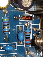
The voltage drop across D7 is way too small - should be about one Vbe (about 0.6V). It goes with the voltage drop across R13 is about zero. 🤔
Let's check Q1. With power off, check both junctions and collector-emitter, each both ways, with a DMM in diode-voltage-drop mode. B-E, B-C should read on Vbe when forward biased and infinity when reverse biased. CE should measure as one Vbe both ways (when the transistor is mounted on this board).
Also, please check the underside of the board around Q1 and its biasing network (R11 R13 R15 D4 C7 C9) for problems.
It is always a good first step after carful Visual examination to go over and look for and reflow all cold solder joints. Always start with the simple things.
Bill
Bill

Hi Alex
What was the reason why you increased C6 and C26 on the SMT version from 330 pf (TH version) to 10n where the other components in the FB network remained the same?
What was the reason why you increased C6 and C26 on the SMT version from 330 pf (TH version) to 10n where the other components in the FB network remained the same?
Both versions have 330pF. It will work with 10nF, too - the difference could not be measured or heard, so we decided to use 330pF to take 10nF off the part list.
Hi Alex,
Makes sense.
Another question, you referred in post 85 that the opamps should preferably have a GBW of 8 - 16 MHz for the FB network as indicated and that faster opamps require that the FB network likely need to be modified. In post 296 you mention a few opamps which a substantially higher GBW. Did you implement a modification when testing the faster opamps mentioned in post 296 or did you use the FB network as is ?
There are no modifications. Faster opamps did not work too well (understandably) on the solderless breadboard, but on the PCB everything from the list works.
Hello;
Any chance to get PCB set (thru-hole; SMT, does not really matter) in any way?
I see that last GB have closed in 1-2 months ago.
regards;
zsolt
Any chance to get PCB set (thru-hole; SMT, does not really matter) in any way?
I see that last GB have closed in 1-2 months ago.
regards;
zsolt
The voltage drop across D7 is way too small - should be about one Vbe (about 0.6V). It goes with the voltage drop across R13 is about zero. 🤔
Let's check Q1. With power off, check both junctions and collector-emitter, each both ways, with a DMM in diode-voltage-drop mode. B-E, B-C should read on Vbe when forward biased and infinity when reverse biased. CE should measure as one Vbe both ways (when the transistor is mounted on this board).
Also, please check the underside of the board around Q1 and its biasing network (R11 R13 R15 D4 C7 C9) for problems.
I've reflowed almost of all components of the malfunctioning channel ... but nothing changed.
I made my multimeter in diode mode and checked B-C, B-E, C-E of Q1, Q2 in both ways.
I don't know well I checked these in proper way.🤔
Q2
B-C 0.625 / 1.966
B-E 0,629 / 1.986 -> 1 (changed immediately)
C-E 0.634 / 0.839
Q1
B-C 0.624 / 1.965
B-E 0,628 / 1.926 -> 1 (changed immediately)
C-E 0.628 / 0.838
Attachments
Last edited:
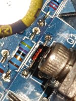
Hoping I might get a bit of help. The negative rail on my through hole Omicron board is shorting to ground. I have gone over the board with a magnifying glass and everything seems to be okay. The diodes and capacitors are installed correctly, as are the transistors and mosfets. I broke D21 while probing around the board checking for continuity. The opamps and comparator have not been installed yet. Any suggestions on where to look?


Thanks in advance.
Dan
Thanks in advance.
Dan
Last edited by a moderator:
It's not easy to see from your photos, but if you haven't checked this already, make sure you have no continuity between the output transistor (Q1, Q2, Q21, Q22) collectors and the heatsink which is earthed. Test both the mounting bolt and pin 2 on each device; if one has shorted, it will short that rail to ground.
- Home
- Amplifiers
- Headphone Systems
- Omicron, a compact headphone amp with -140dB distortion