Hello Quanghao,
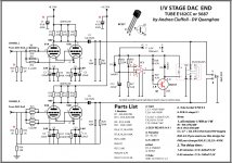
C1 and C7 are the Jensen 47+47uF 450V on the HV P/S board. Correct?
What is the correct value for R30,R31,R32,R33?
Schematic says 470K ???
PCB says 2K ???
You have soldered 2K on your board. Is it correct?
I don't understand that. Please clarify.
Where is R 1 K ???
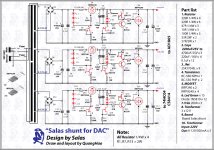
In the Salas shunt Part List: first line 220K 1/4W x 4. Where are they? I can't find them.
R14 Salas shunt schematic should be 220R or 470R?
Thanks
For the I/V stage are C1,C7, No need ( yes Sir)
C1 and C7 are the Jensen 47+47uF 450V on the HV P/S board. Correct?
R30,R31,R32,R33 need for this project!
What is the correct value for R30,R31,R32,R33?
Schematic says 470K ???
PCB says 2K ???
You have soldered 2K on your board. Is it correct?
It seems that the resistors are taken care of by the 200 ohm resistors on DAC board.
I don't understand that. Please clarify.
No after R 200 Ohm, we are have one filter ( chock and C 0.01 + R 1 K)
Where is R 1 K ???
In the Salas shunt Part List: first line 220K 1/4W x 4. Where are they? I can't find them.
R14 Salas shunt schematic should be 220R or 470R?
Thanks
Last edited:
I was actually thinking about using 100uF film cap on C5 and I've actually got one big Solen MKP 100uF 400V at hand I can use. It has to be mounted off board though.
Boy, it must take as much as a pcb space. I didn't know they exist. I suppose they are of the gray kind.
Hello Quanghao,
C1 and C7 are the Jensen 47+47uF 450V on the HV P/S board. Correct?
What is the correct value for R30,R31,R32,R33?
Schematic says 470K ???
PCB says 2K ???
You have soldered 2K on your board. Is it correct?
I don't understand that. Please clarify.
Where is R 1 K ???
In the Salas shunt Part List: first line 220K 1/4W x 4. Where are they? I can't find them.
R14 Salas shunt schematic should be 220R or 470R?
Thanks
I see it's all about language barrier from Quanghao...
I see it's all about language barrier from Quanghao...
Of course, nothing wrong with that, but numbers are not subject to barrier... just matter of accuracy within any level of knowledge I guess.
To reduce the relay delay time at switch on will be changed the RC cell 220K 220uF on Lm311 with 220K 100uF
Hello Quanghao,
C1 and C7 are the Jensen 47+47uF 450V on the HV P/S board. Correct?
What is the correct value for R30,R31,R32,R33?
Schematic says 470K ???
PCB says 2K ???
You have soldered 2K on your board. Is it correct?
I don't understand that. Please clarify.
Hi You can see the circuit diagram is! On standard PC is worth!
I will tell Andrea updat the circuit in the web, you easy to follow
Attachments
All DAC PCB´s are delivered ! I was sent in 28-1-2010
Please keep me informed when they arrived.
Best regards,
Quanghao
Please keep me informed when they arrived.
Best regards,
Quanghao
After many test I consider as the best audio electrolytic capacitors the Jensen.
https://audio.jensencapacitors.com/products/capelyt/elytdual/
These capaciotrs can be buy directly on Ebay shop at:
Jensen 47uf + 47uf 500V Electrolytic Capacitor su eBay.it Electronic Components, Electrical Test Equipment, Business Industrial
Hans Joergen Jensen have confirmed me they original JENSEN caps.
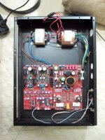
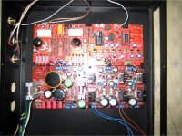
I have do some amendment to Quanghao BOM file. I just follow the figure on PCB photo post by quanghao and schematic by Andrea ciuffoli, I hope it might help some of us to finish the project much easy. Any mistake please let me i will amend it again. Thanks.
https://spreadsheets.google.com/ccc?key=0Al7rXbJqa1XLdE5xdEl6cHVadnlYeWEySEE4dzlrRVE&hl=en
https://spreadsheets.google.com/ccc?key=0Al7rXbJqa1XLdE5xdEl6cHVadnlYeWEySEE4dzlrRVE&hl=en
I have do some amendment to Quanghao BOM file. I just follow the figure on PCB photo post by quanghao and schematic by Andrea ciuffoli, I hope it might help some of us to finish the project much easy. Any mistake please let me i will amend it again. Thanks.
https://spreadsheets.google.com/ccc?key=0Al7rXbJqa1XLdE5xdEl6cHVadnlYeWEySEE4dzlrRVE&hl=en
great! Thank you very much!
Quanghao
you need a "Google account" for accsess. I wish not to acquire an account.... is there anyother way to post it??
Thanks
JD
Thanks
JD
I have do some amendment to Quanghao BOM file. I just follow the figure on PCB photo post by quanghao and schematic by Andrea ciuffoli, I hope it might help some of us to finish the project much easy. Any mistake please let me i will amend it again. Thanks.
https://spreadsheets.google.com/ccc?key=0Al7rXbJqa1XLdE5xdEl6cHVadnlYeWEySEE4dzlrRVE&hl=en
Thank you for posting this. I believe it matches what I have just finished compiling except for R34 on the IV board.The schematic shows a 10R resistor. (New ???)I have do some amendment to Quanghao BOM file. I just follow the figure on PCB photo post by quanghao and schematic by Andrea ciuffoli, I hope it might help some of us to finish the project much easy. Any mistake please let me i will amend it again. Thanks.
https://spreadsheets.google.com/ccc?key=0Al7rXbJqa1XLdE5xdEl6cHVadnlYeWEySEE4dzlrRVE&hl=en
I am assuming that R30-R33 (2k) are needed when used with the DAC END 2. If I am wrong would someone please correct me.
Thanks
Last edited:
Thank you for posting this. I believe it matches what I have just finished compiling except for R34 on the IV board.The schematic shows a 10R resistor. (New ???)
I am assuming that R30-R33 (2k) are needed when used with the DAC END 2. If I am wrong would someone please correct me.
Thanks
I didn't see any R34 on IV board or 10R on IV schematic, can you specify it location?
It seen correct because the R30-R33 in schematic post by quanghao at #426 and on PCB both show 2K.
I just clicked onI didn't see any R34 on IV board or 10R on IV schematic, can you specify it location?
It seen correct because the R30-R33 in schematic post by quanghao at #426 and on PCB both show 2K.
About DAC-END: DAC End 2 - the AD1865N-K with single ended vacuum output stage
At the bottom below R32 and R33 I see on the schematic R34=10R
Best
Bob
I see you used the output inductors whereas andrea did not. any reason?
IMO output chokes on the I/V stage, tybe and brand output capacitors on the tubes, PIO, WIMA Clarity whatever.. are all options available on this good project. It's up to the individual's taste to use the choke or not and the type of tube output capacitors.
At this point of the project you choose what is suitable to your own taste. Try, if you don't like it, change it.
IMO for example I would never put bad polyester cap in parallel with good electrolytic cap (Rifa+++, Silmic++) in series with the cathode of the tube. If someone wants I think it should be MKP. I just leave the elecrolytic alone.
Last edited:
I just clicked on
About DAC-END: DAC End 2 - the AD1865N-K with single ended vacuum output stage
At the bottom below R32 and R33 I see on the schematic R34=10R
Best
Bob
😱Oh! I miss that one, yes R34=10R. Thanks.
- Status
- Not open for further replies.
- Home
- More Vendors...
- Quanghao Audio Design
- OLD THREAD DAC End by Andrea Ciuffoli