Re: Re: Startup circuit
Isolation is not an issue, beacuse the auxiliary winding that takes over powering the PWM IC after the start-up ckt gets things going, is also isolated from the secondary windings. As I understand the original circuit, the PWM IC (an SG3525) is switching all 4 MOSFETs in full-bridge fashion, and is on the primary side of the circuit. Power for the '3525 initially comes from the start-up ckt previously mentioned by chas1, then is replaced by an auxiliary winding that is rectified and filtered just like the secondaries. Feedback from their outputs crosses the galvanic barrier via an optoisolator referenced by a TL431. This is a common method of control, where the PWM control chip is on the primary side and feedback originates on the secondary side.megajocke said:
Doesn't it worry you that there is no isolation between output and input? If you ground the output you'll let out the magic smoke from the startup circuit. And if you don't you might let it out of yourself!
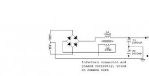
After doing some calculations I got 29uH for output inductor.
Is this for one or value for two?They will be one on each core.
Is this for one or value for two?They will be one on each core.
Inductor value
Luka
The value might be ok depending on your load requirements,
as an example:
switching freq (Fs) = 50kHz
Voltage rail to rail = 80 VDC (+/- 40VDC)
Load current (iL) = 8 amps
Then inductor value would be about (.5 * 80VDC *(1/50kHz) / 8)
my calculator comes up with 100 uH. If you divide that by 2 then you have 50 uH in each rail (+/_) and it is important that they be wound on a single core using bi-filar winding. I wind my own and therefore I tune them by adding or removing turns.
The procedure I use is with an inductance meter I wind turns until I am close to the calculated inductor value and I leave about 4 to 6 inches of wire and connect my inductor to circuit and load test supply using a 400 watt amp I have if things seem ok fine, if not I add or remove turns until amp performs ok. Then with o'scope I check all waveforms under load conditions and then with my DIY load switch I step the load to verify the feedback loop.
As for your question about gauss and telsa it depends on what side of the pond you live on Japan, EU, USA. Just depends on the measurement system you use but they are the same.Read the first few chapter's of Marty Brown's book, he explains it and also shows example's of the different forms for the calculation's.
I have added a picture of the outstage.
chas
Attachments
Re: Re: Re: Startup circuit
The PWM IC is connected to the triangle ground, the output and aux windings are too. But I guess it could be a typo, there would be no need for the optocoupler if the control circuit was connected to the secondary side. BTW, shouldn't the 7812 have a diode between output and input so it doesn't get reverse-biased during startup?
Schematic in this post: Link.
N-Channel said:
Isolation is not an issue, beacuse the auxiliary winding that takes over powering the PWM IC after the start-up ckt gets things going, is also isolated from the secondary windings. As I understand the original circuit, the PWM IC (an SG3525) is switching all 4 MOSFETs in full-bridge fashion, and is on the primary side of the circuit. Power for the '3525 initially comes from the start-up ckt previously mentioned by chas1, then is replaced by an auxiliary winding that is rectified and filtered just like the secondaries. Feedback from their outputs crosses the galvanic barrier via an optoisolator referenced by a TL431. This is a common method of control, where the PWM control chip is on the primary side and feedback originates on the secondary side.
The PWM IC is connected to the triangle ground, the output and aux windings are too. But I guess it could be a typo, there would be no need for the optocoupler if the control circuit was connected to the secondary side. BTW, shouldn't the 7812 have a diode between output and input so it doesn't get reverse-biased during startup?
Schematic in this post: Link.
I am currently doing/building buck converter 42v --> 13-14v, to see how the inductor will respond,waveforms,spikes,...
Then I'll finnish offline one,but I still don't know if my output inductors will be on one core, I guess they could be.
PCB wasn't designed that way, but there won't be any problems.
Then I'll finnish offline one,but I still don't know if my output inductors will be on one core, I guess they could be.
PCB wasn't designed that way, but there won't be any problems.
inductors
Luka
You can use separate inductors, but its is best to use a common one. Inductor value is dependent on input and output voltages so the value for your buck converter will be different than the one you might use in your supply, refer to page 46 of Brown's book.
The formula is below:
L(min) = [Vin(max) - Vout] * T(off) / 1.4 * Iout(min)
Vin(max) = VDC at input to inductor (usually 2 * Vout)
Vout is output voltage
Iout(min) = min load current
T(off) = about 30% 1/fsw
I´m not shure about this 1.4 (constant) in the Inductor equation, but I think the frequency must be 2*fsw for full wave rectifier topologies. It might be considered in that constant, though.
Regards,
Regards,
t(off)
I am not sure what the 1.4 constant includes, but you are correct
that t(off) can be calculated as:
t(off) = 1- (Eout/Ein) / 2 * fsw
I was pointing to a reference in Marty Brown's book for his method for calculating output inductor value's and this is not necessarily the only method.
Thanks for the clearfication and comments
chas1
You're Grounded!
Because the 7812 powers the SG3525 during normal operation, the 7812's ground should be lifted from the secondary ground, and tied to the SG3525's triangle ground. The output secondary's ground should be tied to the Earth ground at the AC input.
There is some confusion with usage of the term "ground", so let me clarify it a bit The DC bulk voltage is about 320V~360VDC wityh respect to its DC-ground (0V) line. The true ground at the AC input ties to the Ground (0V) line of the output voltage(s). In other words, on the primary side we have +320V and 0V; and on the secondary side, we have +55V, GND, and -55V output. The 7812's 0V pin ties to the SG3525's 0V pin and to the DC bulk supply.
Steve
megajocke said:
The PWM IC is connected to the triangle ground, the output and aux windings are too. But I guess it could be a typo, there would be no need for the optocoupler if the control circuit was connected to the secondary side. BTW, shouldn't the 7812 have a diode between output and input so it doesn't get reverse-biased during startup?
Schematic in this post: Link.
Because the 7812 powers the SG3525 during normal operation, the 7812's ground should be lifted from the secondary ground, and tied to the SG3525's triangle ground. The output secondary's ground should be tied to the Earth ground at the AC input.
There is some confusion with usage of the term "ground", so let me clarify it a bit The DC bulk voltage is about 320V~360VDC wityh respect to its DC-ground (0V) line. The true ground at the AC input ties to the Ground (0V) line of the output voltage(s). In other words, on the primary side we have +320V and 0V; and on the secondary side, we have +55V, GND, and -55V output. The 7812's 0V pin ties to the SG3525's 0V pin and to the DC bulk supply.
Steve
Grounds
N-channel
Thanks for the posts about the grounds, The schematic I posted was my design and the ground symbols are not identfied by intention because EU & Far east grounds are different and is left up to the individual to determine the proper grounding for the country that you reside in, if I had indicated the grounding that I use then we would have to describe PCB layout and other items. This is a design that is more or less a copy of an existing working SMPS with a few changes and the PCB layout was my own and has been assembled and is being tested at the present time. I have it powering a 250 watt amp and the listening test is great with full sharp tight bass and no other notable problems. I have however changed a few things and when all doc's are finished , the project is completed I will post the results for anyone who is interested.
Sorry for the confusion, the ground symbols are from my drawing
program.
chas1
chas,
No Problem. 🙂 Always glad to help (or confuse). 😀 Anyway, I just re-read my last post, including the typos. To clarify things even further, the 7812 and '3525 tie their "ground" pins to the 0V line of the DC bulk supply.
I thought I recognized your schematic. Wasn't it from an old version of Popular Electronics? I still have that same issue of it floating around here somewhere, and every now and then think about doing my own version of it.
Steve
article
N-channel
The construction article appeared in "Radio Electronic's" which later became "Electronic's Now" and then "Poptronic's" and then stopped printing.
All the info in on this URL under the K6 Amp, Reinhard Metz , who happens to be a member of this forum did an excellent job in design and documentation of this amplifier. A study of the design of the supply should generate quite a few idea's for DIY. I have noticed and extensive previous post about this supply and some useful mod's for it.
http://www.a-and-t-labs.com
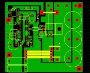
If you see my PCB you will notice in the layout that the input power has its ground, the bulk supply has its ground and the output along with the pwm control is grounded using a large ground plane (copper pour).
chas1
N-channel
The construction article appeared in "Radio Electronic's" which later became "Electronic's Now" and then "Poptronic's" and then stopped printing.
All the info in on this URL under the K6 Amp, Reinhard Metz , who happens to be a member of this forum did an excellent job in design and documentation of this amplifier. A study of the design of the supply should generate quite a few idea's for DIY. I have noticed and extensive previous post about this supply and some useful mod's for it.
http://www.a-and-t-labs.com
If you see my PCB you will notice in the layout that the input power has its ground, the bulk supply has its ground and the output along with the pwm control is grounded using a large ground plane (copper pour).
chas1
Thought it was Radio Electronics, but not sure. Yes, they did have an identity crisis back in the 90's before they went away.
I have seen the K6 Amp and Power Supply. Now that you mention it, I do see the similarities between the two.
If I remember correctly, Reinhard places the whole PWM control on the secondary side, thus enabling direct sensing of the (+/-)outputs, via an LM358 and associated compensation network, and eliminating the need for an optocoupler. Power is supplied to the PWM by a small 50/60Hz housekeeping supply. This also eliminates the need for a bootstrap winding on the main xfmr to power the PWM. The only thing I don't really like about this method is that it will only work on AC, and is not autoranging (you must switch between 115V & 230V- and a switch left in the worng position, ).
This might sound like I'm asking too much, but I would like my design to run on anything from 85-264VAC, and 120-370VDC continuous, with no gaps in coverage. Enter the Active PFC, found in many threads here.
As soon as I get spun up on this ExpressPCB, I am going to start on a schematic for the PFC and PWM. I will most likery separate the two sections for two reasons: 1) Prevention of beat frequencies between the PFC and PWM; and 2) Modularity of the design, enabling me to change parts without having to change the whole circuit. I mentioned this about two pages bcak in this thread.
I have seen the K6 Amp and Power Supply. Now that you mention it, I do see the similarities between the two.
If I remember correctly, Reinhard places the whole PWM control on the secondary side, thus enabling direct sensing of the (+/-)outputs, via an LM358 and associated compensation network, and eliminating the need for an optocoupler. Power is supplied to the PWM by a small 50/60Hz housekeeping supply. This also eliminates the need for a bootstrap winding on the main xfmr to power the PWM. The only thing I don't really like about this method is that it will only work on AC, and is not autoranging (you must switch between 115V & 230V- and a switch left in the worng position,
).This might sound like I'm asking too much, but I would like my design to run on anything from 85-264VAC, and 120-370VDC continuous, with no gaps in coverage. Enter the Active PFC, found in many threads here.
As soon as I get spun up on this ExpressPCB, I am going to start on a schematic for the PFC and PWM. I will most likery separate the two sections for two reasons: 1) Prevention of beat frequencies between the PFC and PWM; and 2) Modularity of the design, enabling me to change parts without having to change the whole circuit. I mentioned this about two pages bcak in this thread.
schematic
Luka
I will be glad to post the finished schematic after all testing is complete. At the current time I am testing a full bridge using current control and I will start testing the halfbridge in the next week and both of them should be finished within two weeks. Are your testing your buck converter?
chas1
Can't since I dont have Inductance meter yet to get right value, but I will do that shortly.Can't wait to see final ver. of your supply.Pic and sch, maybe even the pcb...
Few questions about mc34025 for you chas:
1.)why did you put 1k resistor betwen pin 7 and 9?
2.)I don't intend to connect pin 3 to 1.Is that OK?
3.)Is that 150ohm resistor for current limit 0.25w or higher
4.)what is turn ratio, if you want to limit secundary current to 65A max?
1.)why did you put 1k resistor betwen pin 7 and 9?
2.)I don't intend to connect pin 3 to 1.Is that OK?
3.)Is that 150ohm resistor for current limit 0.25w or higher
4.)what is turn ratio, if you want to limit secundary current to 65A max?
- Home
- Amplifiers
- Power Supplies
- Offline full-bridge SMPS… need help