Or can one get himself the Booster O2?
Which is his price for EU
Hi! The at-cost price for anyone registered here on the forum is $14 for the bare board, which comes with the 4 sets of connection pins, and 26AWG silicon connection. The board is ENIG (gold) finish. Plus actual shipping cost, I can get a quote from the post office. I'll send you a PM with more information. 🙂
15uV and 2uV DC output offset!
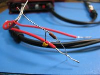
I just had to share the picture below. This is from an new V3.5 O2 Booster Board installed in a fellow's O2 headphone amp. The 1R output resistors on the O2 board have been removed and replaced with jumper wires (remember the Booster Board does not need any series output resistors). 15 micovolts and 2 microvolts DC output offset on the two channels and it doesn't change a bit with the amp's volume control rotated from one end to the other. 😀 You have to love the OPA827.
There is some thermal drift over time but it is small, usually in the +/-30uV region.
Attachments

Last edited:
Ok after building two O2's, and ODA,and inverting O2, and three Super Cmoys I am finally going to build the O2 Booster Board!! Ha!
Parts on order!!
Alex
Parts on order!!
Alex
Here it is:
Started this morning at 9 am 'ish and finished up around 3pm with lunch and a couple of eye "strain" breaks!! LOL!
It didnt work the first time and I was abit depressed about that! No sound from the left channel and a lous AC "buzz" sound on the right channel but not clear.
Upon closer inspection one of the 827 (IC3) was not as well soldered as I first thought!! had to reflow a few times pins 1,2,3 and this fixed the issue!! Yeah!
It sounds real good so far, but I havent done a rea subjective test listen session yet, I am beat after soldering all those tiny SMD parts!! ha!
It wasnt that hard, the hard part is geting the parts out of the plastic bags and plastic containers...and NOT loosing them or dropping them on the floor!!
Also the parts being so small can be prone to overheating when soldering so its a balancing act, this is what caused my issue with the mis-soldered 827.
Hope to get to a good listening session against a stock JDS labs O2 tomorrow.
Alex
Attachments
Ok we have spent the morning listening to a normal O2 vs the O2 with a booster board.
I setup the two amps with my SPL meter with a 1Khz test tone to 85db. If you fiddle with the volume knob its easy to get confused and make an amp that doesnt sound that good a whole lot better....
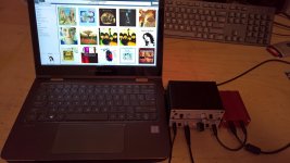
The source was an HP Spectre laptop to a ODAC to the amps. The music player I used was JRiver running in Bitperfect mode setup. The OS on the laptop is Win10 with all the updates, drivers etc...
I used my reference Beyerdynamics T90's (250 ohm) and a set of Audio Technica MSR7's (35 ohm, 100 dB/mW sensitivity). The sensitivity for the T90's: 102 dB SPL at 500 Hz at 1 mW. (1 mW is 500 mV at 250 Ω, thus 1V is 4 mW or +6 dBm into 250 Ω, so 1V gives 108 dB SPL. From Ken Rockwell.com review).
I am a pretty objective analytical person and dont believe in a lot of the snake oil that out there all over the audio world. Many of the amps I have built in the past few years all sound pretty good with subtle differences on the audio side and vast differences on the versatility side....mostly mechanical connections etc.
That said, as I listened to both my objective side was telling me that there isnt a lot of differences between the two...but subjectively I was drawn to the Booster board O2 again and again. It seems to be "clearer, more open, beautiful bass response and all the details in the background were there in spades. I played many very well recorded songs that I am very familiar with, and even though the O2 was excellent the O2 with booster board just drew me to its sound....could very well be subjective bias in my brain, but I do know that the booster board does not hurt or impair the O2 in anyway.
I am wondering if the slew rates have anything to do with this?
The major thing I noticed is the volume knob setting on both varied alot with the two headphones. The 35 Ohm MSR7's did not need much volume pot rotation at all around 8-9 o'clock, the T90s 250 ohm cans needed a lot more rotation to get the 85db, around 10 o'clock position.
What was immediately noticed it the turn on thump is gone...the booster board is totally silent and has a "black background". With the volume all the way up there is no hiss, hum or noise of anykind.
The amp comes alive around 3 seconds and even with the music source hot the turn on is smooth and not abrupt.
So all in all the booster board is a great upgrade for the Original O2 and sounds well "transparent", "open", "natural, and .......all those other subjective adjective!
Great job AGDR!!
Alex
I setup the two amps with my SPL meter with a 1Khz test tone to 85db. If you fiddle with the volume knob its easy to get confused and make an amp that doesnt sound that good a whole lot better....
The source was an HP Spectre laptop to a ODAC to the amps. The music player I used was JRiver running in Bitperfect mode setup. The OS on the laptop is Win10 with all the updates, drivers etc...
I used my reference Beyerdynamics T90's (250 ohm) and a set of Audio Technica MSR7's (35 ohm, 100 dB/mW sensitivity). The sensitivity for the T90's: 102 dB SPL at 500 Hz at 1 mW. (1 mW is 500 mV at 250 Ω, thus 1V is 4 mW or +6 dBm into 250 Ω, so 1V gives 108 dB SPL. From Ken Rockwell.com review).
I am a pretty objective analytical person and dont believe in a lot of the snake oil that out there all over the audio world. Many of the amps I have built in the past few years all sound pretty good with subtle differences on the audio side and vast differences on the versatility side....mostly mechanical connections etc.
That said, as I listened to both my objective side was telling me that there isnt a lot of differences between the two...but subjectively I was drawn to the Booster board O2 again and again. It seems to be "clearer, more open, beautiful bass response and all the details in the background were there in spades. I played many very well recorded songs that I am very familiar with, and even though the O2 was excellent the O2 with booster board just drew me to its sound....could very well be subjective bias in my brain, but I do know that the booster board does not hurt or impair the O2 in anyway.
I am wondering if the slew rates have anything to do with this?
The major thing I noticed is the volume knob setting on both varied alot with the two headphones. The 35 Ohm MSR7's did not need much volume pot rotation at all around 8-9 o'clock, the T90s 250 ohm cans needed a lot more rotation to get the 85db, around 10 o'clock position.
What was immediately noticed it the turn on thump is gone...the booster board is totally silent and has a "black background". With the volume all the way up there is no hiss, hum or noise of anykind.
The amp comes alive around 3 seconds and even with the music source hot the turn on is smooth and not abrupt.
So all in all the booster board is a great upgrade for the Original O2 and sounds well "transparent", "open", "natural, and .......all those other subjective adjective!
Great job AGDR!!
Alex
Attachments
Alex, thanks for the review! You are very thorough with your reviews. I know takes a lot of time to set everything up and do the A/B with a lot of different music types.
One of primary goals with the Booster Board is what they say in medical school, "first do no harm". 🙂 Wouldn't want to make any of the measurements or the listening experience with NwAvGuy's wonderful O2 worse in any way.
I've formed the opinion over the years that anything which gets the NJM4556A chips out of the (O2) box is a good thing. mlackey's post in the O2 thread about replacing them with the OPA1688 is really interesting. That may solve the "NJM4556A problem" for folks whose headphones and cables don't pose a big capacitive load, plus it reduces that big 3mV DC offset of the NJM4556A by an order of magnitude, similar to the Booster Board. Of course to that the Booster Board adds twice the peak current output, zero ohms out (if the O2 1R resistors are shorted), the anti-thump relay, power rail leds, reverse rail clamps, and isolation filters on the OPA827 power rails. But all of that is less important than fixing the bass problem with the NJM4556A by replacing it, either with the Booster's OPA827 + LME49600 or the OPA1688.
On the slew rate, NwAvGuy in his blog says that since the recording chain at the studios limits slew to around 2V/uS even the 3V/uS in the NJM4556A is enough. But I know a lot of folks out there believe they can hear a difference with a higher slew.
Thanks again for the review!
Last edited:
I have to agree hear on the 4556's...theres definitely something going on here, I listened again for a few hours and I definitely think the sound presentation is different from an O2 in a good way. The only way to describe the difference is with subjective adjectives.The sound is clearer, cleaner, more easy to dig into the details with a good set of headphones.
If I were to listen the booster board version would be my first pick.
I have not jumpered out the 1 ohm resistors but think I will try this in the next few days as well.
Alex
If I were to listen the booster board version would be my first pick.
I have not jumpered out the 1 ohm resistors but think I will try this in the next few days as well.
Alex
I have not jumpered out the 1 ohm resistors but think I will try this in the next few days as well.
Alex
Recommended! That is one of the big benefits of the Booster Board, a single chip output so no need for balancing resistors. Jumper those 1Rs and enjoy zero ohm output. 🙂
Does the booster affect the optimum gain of 1x/3.3x?
If you have 1x/3.3x now you will still have that with the Booster. The voltage gain is still controlled by the first stage in the O2.
Measurements on a new version, V3.6, part 1
Here are some measurements on a brand new version of the O2 Booster Board, V3.6, with some minor changes from the previous V3.5. I've listed the changes in the first post in this thread, along with links to the project materials on Google Drive - BOM, build instructions, schematic, layout, part ID diagram, installation instructions, and photos. 🙂
CHiroshsi - great suggestion in the other thread about hiring tomchr make some measurements with his AP on the Booster Board since he is offering that consulting service. I'm chatting with him now to set that up. I just wanted to run a bunch of tests myself first on this new version to catch any "new version" surprises before the AP work. 🙂
Photos:
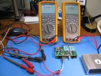
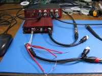
The first 4857 is the test setup. A NwAvGuy O2 with the V3.6 Booster Board plugged in and slid into the top slot of the case. The analyzer is one of the "toy" QA401 boxes, essentially a (fairly good, calibrated) sound card in a box. The "red" end of the breakout cable is the right channel while the white is the left, standard audio color code. I have verified both cables really are wired that way - lol, I've run into that particular manufacturing defect before. All the measurements here are taken with two "throw away" (primary) brand new 9V cells powering the boards. The blue mat is a grounded anti-static mat.
The next photo is a close up of the load that I move between the channels. The load resistor is 32 ohm, 1/2W, 0.1% and the capacitor, which I add in some tests below as noted, is a 680pF 5% C0G MLCC.
The next 4 photos are IC temperature checks, for oscillation. These are done with a 0dBV (1Vrms) signal in and out, with the 32R load and with the 680pF capacitor attached. The unit had been running about 5 minutes when these were taken. The first two are the OPA827 chips on the two channels, then one of the LME49600 buffers (I measured both and they were nearly identical). The final temperature reading is a 12V SMD regulator which powers the headphone relay circuit. Note that since all of these measurements are done on batteries the temperatures will be less than with the +/-12Vdc power rails. I hope to have some time today to make some AC-powered measurements. But the important thing here is the temperatures are all around 95F, not the 130 - 160F+ I would expect to see with oscillation going on. Hard to read on the display but these are all F and not C, of course.
Tests...
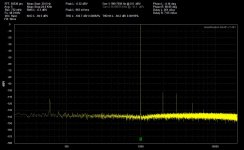
The first two are loopback tests on the QA401 since it is known to have some 2nd and 3rd harmonic challenges at higher levels (the ADC they used, apparently). The first is at -10dBV (around 300mVrms) as shown at the top of the graph, while the second is at 0dBV (around 1Vrms). I picked these two levels based on the excellent comments tomchr made in his O2 measurement thread. The -10dBV is the "flea power" level NwAvGuy used in his dScope measurements, while the 0dBV level is a more real-world level for headphones that actually need a headphone amplifier. Like jcx pointed out in that thread, many modern high sensitivity cans and IEMs simply don't require a headamp anymore.
The other test conditions are in the upper left corner of the plots. And again all of these are done with the O2+Booster Board running on primary 9V batteries, so +/-9V rails.
The final two are the THD+N plots at -10dBV on the right and left channels with the purely resistive 32R load. Remember you have to subtract out those substantial 2nd and 3rd harmonic lines internal to the QA401 tester, shown in the loopback plot. The Booster Board appears to be doing extremely well here. The power line harmonics are all EMI pickup since it is running on batteries and I don't have the front and rear panels on the O2 case here.
Out of photo posting slots, on to part 2....
Clicking on the arrows in the lower left of the photos will zoom them up. Hovering the mouse over them will bring up the photo number.
Here are some measurements on a brand new version of the O2 Booster Board, V3.6, with some minor changes from the previous V3.5. I've listed the changes in the first post in this thread, along with links to the project materials on Google Drive - BOM, build instructions, schematic, layout, part ID diagram, installation instructions, and photos. 🙂
CHiroshsi - great suggestion in the other thread about hiring tomchr make some measurements with his AP on the Booster Board since he is offering that consulting service. I'm chatting with him now to set that up. I just wanted to run a bunch of tests myself first on this new version to catch any "new version" surprises before the AP work. 🙂
Photos:
The first 4857 is the test setup. A NwAvGuy O2 with the V3.6 Booster Board plugged in and slid into the top slot of the case. The analyzer is one of the "toy" QA401 boxes, essentially a (fairly good, calibrated) sound card in a box. The "red" end of the breakout cable is the right channel while the white is the left, standard audio color code. I have verified both cables really are wired that way - lol, I've run into that particular manufacturing defect before. All the measurements here are taken with two "throw away" (primary) brand new 9V cells powering the boards. The blue mat is a grounded anti-static mat.
The next photo is a close up of the load that I move between the channels. The load resistor is 32 ohm, 1/2W, 0.1% and the capacitor, which I add in some tests below as noted, is a 680pF 5% C0G MLCC.
The next 4 photos are IC temperature checks, for oscillation. These are done with a 0dBV (1Vrms) signal in and out, with the 32R load and with the 680pF capacitor attached. The unit had been running about 5 minutes when these were taken. The first two are the OPA827 chips on the two channels, then one of the LME49600 buffers (I measured both and they were nearly identical). The final temperature reading is a 12V SMD regulator which powers the headphone relay circuit. Note that since all of these measurements are done on batteries the temperatures will be less than with the +/-12Vdc power rails. I hope to have some time today to make some AC-powered measurements. But the important thing here is the temperatures are all around 95F, not the 130 - 160F+ I would expect to see with oscillation going on. Hard to read on the display but these are all F and not C, of course.
Tests...
The first two are loopback tests on the QA401 since it is known to have some 2nd and 3rd harmonic challenges at higher levels (the ADC they used, apparently). The first is at -10dBV (around 300mVrms) as shown at the top of the graph, while the second is at 0dBV (around 1Vrms). I picked these two levels based on the excellent comments tomchr made in his O2 measurement thread. The -10dBV is the "flea power" level NwAvGuy used in his dScope measurements, while the 0dBV level is a more real-world level for headphones that actually need a headphone amplifier. Like jcx pointed out in that thread, many modern high sensitivity cans and IEMs simply don't require a headamp anymore.
The other test conditions are in the upper left corner of the plots. And again all of these are done with the O2+Booster Board running on primary 9V batteries, so +/-9V rails.
The final two are the THD+N plots at -10dBV on the right and left channels with the purely resistive 32R load. Remember you have to subtract out those substantial 2nd and 3rd harmonic lines internal to the QA401 tester, shown in the loopback plot. The Booster Board appears to be doing extremely well here. The power line harmonics are all EMI pickup since it is running on batteries and I don't have the front and rear panels on the O2 case here.
Out of photo posting slots, on to part 2....
Clicking on the arrows in the lower left of the photos will zoom them up. Hovering the mouse over them will bring up the photo number.
Attachments
-
 tester loopback -10dBV.jpg146.8 KB · Views: 129
 -
 tester loopback 0dBV.jpg144.9 KB · Views: 122
 -
 32R load -10dBV red.jpg146.3 KB · Views: 123
 -
 32R load -10dBV white.jpg146.7 KB · Views: 112
 -
 IMG_4864.JPG462 KB · Views: 121
 -
 IMG_4861.JPG412.8 KB · Views: 258
 -
 IMG_4862.JPG425.7 KB · Views: 266
 -
 IMG_4860.JPG458.5 KB · Views: 268
 -
 IMG_4858.JPG402.2 KB · Views: 262
 -
 IMG_4857.JPG543.8 KB · Views: 276
Last edited:
Measurements on a new version, V3.6, part 2
continued from above...
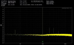
The next group of plots are now with 0dBV in and out, around 1Vrms. The first two are with a purely resistive 32R load for the right and left channels. The third is with the 680pF capacitor added to the 32R, on the right channel.
Remember again that the 2nd, 3rd, and now 5th and 7th harmonics (due to the higher signal levels, of course) generated by the analyzer itself, in that 0dBV loop-back plot in the post above, have to be subtracted out. I've attached a copy of that loop-back plot here as the last graph, for reference. Total THD+N is calculated by the analyzer in all cases at the top of the graph, in the middle.
Clicking on the arrows in the lower left of the photos will zoom them up. Hovering the mouse over them will bring up the photo number.
continued from above...
The next group of plots are now with 0dBV in and out, around 1Vrms. The first two are with a purely resistive 32R load for the right and left channels. The third is with the 680pF capacitor added to the 32R, on the right channel.
Remember again that the 2nd, 3rd, and now 5th and 7th harmonics (due to the higher signal levels, of course) generated by the analyzer itself, in that 0dBV loop-back plot in the post above, have to be subtracted out. I've attached a copy of that loop-back plot here as the last graph, for reference. Total THD+N is calculated by the analyzer in all cases at the top of the graph, in the middle.
Clicking on the arrows in the lower left of the photos will zoom them up. Hovering the mouse over them will bring up the photo number.
Attachments


Last edited:
That is great news! Really looking forward to read tomchr's results and impressions. Ideally you want him to take the measurements of a booster board installed in his O2, but maybe he is not ready to mod it?
Skickat från min Nexus 5X via Tapatalk
Skickat från min Nexus 5X via Tapatalk
That is great news! Really looking forward to read tomchr's results and impressions. Ideally you want him to take the measurements of a booster board installed in his O2, but maybe he is not ready to mod it?
Finally someone who can make AP measurements on O2-related things! Tom wants me to send him a Booster Board installed in an O2 and ready to go, so will do. I'll build the O2 board up with NwAvGuy's standard BOM, none of the part upgrades or mods I have listed out on my website. I'll build it up for 1x/2.5x gain.
Tom has confirmed that the AP doesn't have the problem the QA401 does with the internally-generated harmonics. Completely clean. 🙂
I'm putting together a list of tests for Tom to run. THD+N at -10 dBV and 0dBV into the typical range of headphone loads has to be in there at a minimum. I'll look through the bunch of tests NwAvGuy did. If anyone has suggestions on tests to run, please post!
I'm going to run and post an additional set of QA401 tests with a 16 ohm load running on 9V primary cells. At 0 dBV that would be 1Vrms/16 = 63mA(rms) and 89mA(peak) per channel for 16R. Looks like 9V primary cells are easily good for 100mA, given that I'm only testing one channel at a time:
Discharge tests and capacity measurement of 9 volt transistor radio batteries at high current, 100mA to 500mA engineering data
I had a bit of laugh looking at the top 9V battery discharge curve. That little piece of grey trace all the way over on the left axis is a 9V carbon-zinc cell he threw in there for fun, along with the alkaline cells.
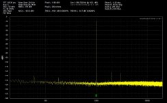
O2 on AC - Booster Board THD+N tests V3.6, part 1
So here are a bunch of tests with the O2 + Booster Board running on AC (12Vac 1000mA wall transformer). Thinking about it a bit more (from my comments above), running the 16 ohm load test on batteries wouldn't really provide any more information vs. just doing it here, on AC. All of the tests below are with the O2 (and Booster Board) on AC.
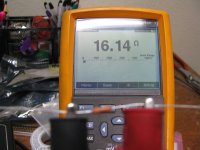
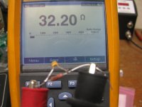
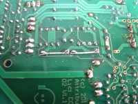
The first two photos are proof of the loads being used. These are the same series of Vishay 0.1% 1/2W resistor. The test leads in the Fluke are about 0.14 ohms, which is why those extra digits even though a 0.1% resistor. The DMM has a relative reading mode I could have used to subtract the lead resistance out, but I forgot about it.
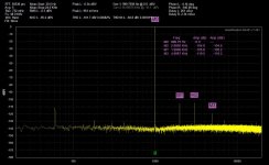
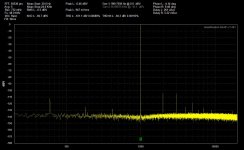
The next two are THD+N plots of the (32 ohms + 680pF) load at 0dB (1Vrms) in and out. Then the 16 ohms purely resistive load at 0dB. Remember you have to subtract out the substantial internal 2nd, 3rd, 5th, and 7th harmonics from the QA401 analyzer, shown in the 0dB loopback graph in the previous post.
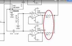
Next are tests with another fun thing you can do with the Booster Board, 0 ohms output. 😀 With the Booster plugged into the O2 board, in place of U3 and U4, the 1 ohm O2 output balancing resistors are still in place. Those resistors have to be there for the paralleled op-amp sections on the stock O2, but are not needed with the Booster's single LME49600 output chip. They just wind up in parallel and are 0.5 ohms in series with the Booster output. The result is the same 0.5 ohms output resistance the stock O2 has.
But those 1R resistors (the O2's R10, R11, R15, & R18) can simply be jumpered straight across on the back of the O2 board to yield a true zero ohm output resistance for the Booster board. That is zero ohms thanks to the negative feedback of course, not zero ohms in the LME49600 chips per se. A couple of different folks who have built up Booster Boards have told me the specific reason they were interested is the zero ohms out option. 🙂 Please remember that if you ever then remove the Booster Board from your O2 and plug the original NJM4556A chips back in for U3 and U4, you must remove those jumpers on the 1R resistors so the chip halves can current-balance properly.
The next two photos shows the 1R resistors on the left channel, the O2's R15 and R18, shorted across. The tests above were on the O2+Booster right channel. I switched to the left just because those 1R resistors were a bit easier to get to on the back of the board.
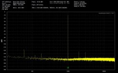
The next two graphs show the results on the O2+Booster left channel, 16R load and 0dBV, now first with the two 1Rs in place on the O2 board (0.5R Zout) and then with them shorted across (0R Zout). And the final two show the same thing with the load now swapped for the 32R+680pF, 0.5R Zout and 0R Zout. Again remember to subtract out all the QA401 inherent harmonics in the 0dBV loop-back plot in the post above.
And a possible point of confusion: we are moving from the right to the left channel on the O2+Booster here, the device under test, but continuing to use the left channel on the analyzer for everything. That is why all the plots are in yellow, which is the left channel on the QA401. At 48K sampling rate the left and right channels of the QA401 are virtually identical. Lol, not so at 192Ksps, but that is another story (a known QA401 issue).
Clicking on the arrows in the lower left of the photos will zoom them up. Hovering the mouse over them will bring up the photo number.
So here are a bunch of tests with the O2 + Booster Board running on AC (12Vac 1000mA wall transformer). Thinking about it a bit more (from my comments above), running the 16 ohm load test on batteries wouldn't really provide any more information vs. just doing it here, on AC. All of the tests below are with the O2 (and Booster Board) on AC.
The first two photos are proof of the loads being used. These are the same series of Vishay 0.1% 1/2W resistor. The test leads in the Fluke are about 0.14 ohms, which is why those extra digits even though a 0.1% resistor. The DMM has a relative reading mode I could have used to subtract the lead resistance out, but I forgot about it.
The next two are THD+N plots of the (32 ohms + 680pF) load at 0dB (1Vrms) in and out. Then the 16 ohms purely resistive load at 0dB. Remember you have to subtract out the substantial internal 2nd, 3rd, 5th, and 7th harmonics from the QA401 analyzer, shown in the 0dB loopback graph in the previous post.
Next are tests with another fun thing you can do with the Booster Board, 0 ohms output. 😀 With the Booster plugged into the O2 board, in place of U3 and U4, the 1 ohm O2 output balancing resistors are still in place. Those resistors have to be there for the paralleled op-amp sections on the stock O2, but are not needed with the Booster's single LME49600 output chip. They just wind up in parallel and are 0.5 ohms in series with the Booster output. The result is the same 0.5 ohms output resistance the stock O2 has.
But those 1R resistors (the O2's R10, R11, R15, & R18) can simply be jumpered straight across on the back of the O2 board to yield a true zero ohm output resistance for the Booster board. That is zero ohms thanks to the negative feedback of course, not zero ohms in the LME49600 chips per se. A couple of different folks who have built up Booster Boards have told me the specific reason they were interested is the zero ohms out option. 🙂 Please remember that if you ever then remove the Booster Board from your O2 and plug the original NJM4556A chips back in for U3 and U4, you must remove those jumpers on the 1R resistors so the chip halves can current-balance properly.
The next two photos shows the 1R resistors on the left channel, the O2's R15 and R18, shorted across. The tests above were on the O2+Booster right channel. I switched to the left just because those 1R resistors were a bit easier to get to on the back of the board.
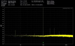
The next two graphs show the results on the O2+Booster left channel, 16R load and 0dBV, now first with the two 1Rs in place on the O2 board (0.5R Zout) and then with them shorted across (0R Zout). And the final two show the same thing with the load now swapped for the 32R+680pF, 0.5R Zout and 0R Zout. Again remember to subtract out all the QA401 inherent harmonics in the 0dBV loop-back plot in the post above.
And a possible point of confusion: we are moving from the right to the left channel on the O2+Booster here, the device under test, but continuing to use the left channel on the analyzer for everything. That is why all the plots are in yellow, which is the left channel on the QA401. At 48K sampling rate the left and right channels of the QA401 are virtually identical. Lol, not so at 192Ksps, but that is another story (a known QA401 issue).
Clicking on the arrows in the lower left of the photos will zoom them up. Hovering the mouse over them will bring up the photo number.
Attachments
-
 IMG_4870.JPG493.4 KB · Views: 104
 -
 IMG_4871.JPG445.2 KB · Views: 102
 -
 32R+680pF load 0dBV red.jpg154.5 KB · Views: 115
 -
 16R load 0dBV red.jpg146.1 KB · Views: 135
 -
 O2 1R balancing resistors.JPG67.5 KB · Views: 117
 -
 IMG_4888.JPG559.9 KB · Views: 118
 -
 16R load 0dBV 0.5R output white.jpg146 KB · Views: 128
 -
 16R load 0dBV 0R output white.jpg146.1 KB · Views: 118
 -
 32R+680pF load 0dBV 0.5R output white.jpg146 KB · Views: 104
 -
 32R+680pF load 0dBV 0R output white.jpg145.6 KB · Views: 107
Last edited:
O2 on AC - Booster Board THD+N tests V3.6, part 2
Continued from above...
Since the O2+Booster combination is now running on AC the rails have gone up to +/-12Vdc from the previous +/-9Vdc on batteries. So it seemed that some new part temperature measurements are in order, especially since some of the tests now involve the 16 ohm load, plus this is all pure sine wave testing. Remember that with actual music "music power" applies, where the average levels will typically be 1/2 to 1/3 the peak. But with sine wave testing you have maximum all the time. Recall that even in NwAvGuy's O2 writeup he says that the O2 should be allowed to cool off (the NJM4556A output chips) after every 10 minutes or so of sine wave testing at high(er) levels with a 16R load.
Same applies here, although from the readings below it looks like at just 0dBV (1Vrms) the Booster Board is OK with continuous sine wave testing at 16R. Higher levels would require a cooling off period. But again... not with music unless you are running it at very high levels, with music that has high sustained peaks, and with 16 ohm headphones or IEMs.
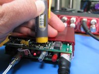
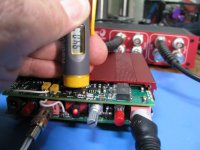
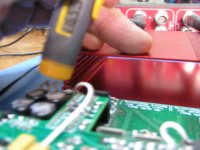
The first photo shows a steady-state temperature on the LME49600 chips with a 16R load and 0dBV, about 112F, which is fine. Remember that NwAvGuy actually stated once that 150F on the regulator chips was OK, since the maximum based on junction temperature was around 180F. 😛 Umm..... The next shows the O2's regulators, about 116F. Sorry about the blurry photo! The current through the regulators (and the LME49600 buffer chip on the left channel with the 16R load) is around 1Vrms/16R = 63mA(rms) = 90mA(peak). For the regulators add about 25mA of chip idle current to that, around 88mA(rms). The batteries are out, so no additional battery charging current.
Next is the OPA827 steady-state, about 106F, which is fine.
Continued from above...
Since the O2+Booster combination is now running on AC the rails have gone up to +/-12Vdc from the previous +/-9Vdc on batteries. So it seemed that some new part temperature measurements are in order, especially since some of the tests now involve the 16 ohm load, plus this is all pure sine wave testing. Remember that with actual music "music power" applies, where the average levels will typically be 1/2 to 1/3 the peak. But with sine wave testing you have maximum all the time. Recall that even in NwAvGuy's O2 writeup he says that the O2 should be allowed to cool off (the NJM4556A output chips) after every 10 minutes or so of sine wave testing at high(er) levels with a 16R load.
Same applies here, although from the readings below it looks like at just 0dBV (1Vrms) the Booster Board is OK with continuous sine wave testing at 16R. Higher levels would require a cooling off period. But again... not with music unless you are running it at very high levels, with music that has high sustained peaks, and with 16 ohm headphones or IEMs.
The first photo shows a steady-state temperature on the LME49600 chips with a 16R load and 0dBV, about 112F, which is fine. Remember that NwAvGuy actually stated once that 150F on the regulator chips was OK, since the maximum based on junction temperature was around 180F. 😛 Umm..... The next shows the O2's regulators, about 116F. Sorry about the blurry photo! The current through the regulators (and the LME49600 buffer chip on the left channel with the 16R load) is around 1Vrms/16R = 63mA(rms) = 90mA(peak). For the regulators add about 25mA of chip idle current to that, around 88mA(rms). The batteries are out, so no additional battery charging current.
Next is the OPA827 steady-state, about 106F, which is fine.
Attachments


Last edited:
- Home
- Amplifiers
- Headphone Systems
- O2 headamp output booster PCB