I use 60R on the primary of my Sowter I/V transformers for my balanced dual 1541 DAC and can then experiment with secondary resistors.
A member on here (Chiurutu) has a balanced 1541 dac board on ebay: https://www.ebay.co.uk/itm/325473063909 for anyone who wishes to hear the benefits of balanced operation.
A member on here (Chiurutu) has a balanced 1541 dac board on ebay: https://www.ebay.co.uk/itm/325473063909 for anyone who wishes to hear the benefits of balanced operation.
Hi Ben and batteryman
I don’t want to derail peppe’s thread completely.
It’s supposed to be about the D1/Zen i/v stage…and I was wondering if the D1/Zen was a better (read simpler) solution for me since I’m struggling with what to do about the insufficient output on my D3/TDA1541 based DAC.
I’m completely inexperienced with the use of these DAC transformers and i/v stages in general…however, my thinking was what Ben concluded.
These transformers were wound by bisesik.
I’ve posted in his thread requesting further guidance to this dilemma…but haven’t heard anything yet.
I was under the impression these transformers were an optimal solution for running a differential arrangement with the tda1541…but I just don’t understand how that is the case when they would result in such a high output impedance.
It may be that the original owner requested they were wound like this for some reason…but it escapes me.
My head is kind of hurting from trying to figure out how I would use them.
ECDesign’s advice on passive i/v stages that I came across was:
“If I -had- to make a -fully- passive I/V stage for the TDA1541A I would do following:
1) Resistive divider that provides +240mV. For example 24 Ohms in series with 476 Ohms connected to the +5V supply and a suitable electrolytic cap (1000uF/6V3 for example) in parallel with 24 Ohms.
0.002mA bias current results in 240mV drop across a 120R resistor. Without further action we would end up with -0.24V DC offset on the I/V resistor and on the connected transformer. By lifting the I/V resistor GND reference to +0.24V this DC offset voltage is nulled (-0.24V) + (+0.24V) = 0. And this can still be achieved with passive components (2 resistors and a capacitor).
2) Connect a 120R Welwyn W21 wire wound resistor between +240mV and TDA1541A output. With TDA1541A full scale current of 4mA this results in 480mVpp. This is still below the clipping limit of around 600mVpp and distortion stays below the audibility threshold of roughly 1%. It is -very- important to use a low noise wire wound (not bulk metal foil !!) resistor here. Welwyn W21 and Rhopoint econister are recommended.
3) Connect a good quality 1:4 step up transformer to the 120R resistor (LL1674 for example). Use a transformer that works optimal with a source load of around 100 … 200 Ohms.
4) Connect a RC filter to the transformer secondary to suppress ringing (use test signal and scope to tune).
You will then have a fully passive I/V stage that provides 1.92Vpp and an output impedance of approx. 1900 Ohms (120R * 4 * 4).
Low passive I/V resistor values give lowest distortion but poor resolution as most of the LSBs are burried deep below the noise floor.
With 12.5 Ohm passive I/V resistor (50mVpp) LSB is only 0.05 / 65536 = 762 nanovolts. Noise levels of up to 1 millivolts in an I/V stage are quite common. So 6 MSBs will stay above the noise floor while the other 10 hide below it. Suppose one could still hear signals that are below the noise floor one might just be able to squeeze out 8 bits resolution”
Additionally I came across this information posted by ECDesigns while trying to figure out if a different arrangement in simultaneous mode would work for me:
“If you already have LE, BCK, DL and DR,
(1) SE mode: feed these 4 signals to one chip.
(2) Parallel mode: feed LE, BCK, DL, DL to left channel chip, feed LE, BCK, DR, DR to right channel chip.
(3) Balanced mode (simplified, not fully correct): feed LE, BCK, DL, -DL (inverted DL) to left channel chip, feed LE, BCK, DR, -DR (inverted DR) to right channel chip.
For SE mode use one I/V resistor and +2mA bias source or active I/V converter circuit on each output.
For parallel mode you can parallel the outputs on each chip and use an I/V resistor with half the usual value and +4mA bias or active I/V converter circuit. Full scale current doubles to -8mA!
For balanced mode you can use a separate I/V resistor on each output and +2mA bias source for each of the 4 resistors. You can also use 4 separate active I/V converter circuits.
The balanced outputs can be fed directly into the balanced inputs of a (pre) amp, suitable step-up transformer with twin primary windings providing SE output & balanced output, or summing stage.”
I believe Ryan was familiar with this information when he designed the D3 project. I also believe he was using a low ratio (like 1:4) transformer at some point.
@batteryman
I’m not knowledgeable enough to understand what affect having a resistor on the primary and secondary has on the performance of a passive i/v transformer…or if its even possible/advisable with the transformers I have.
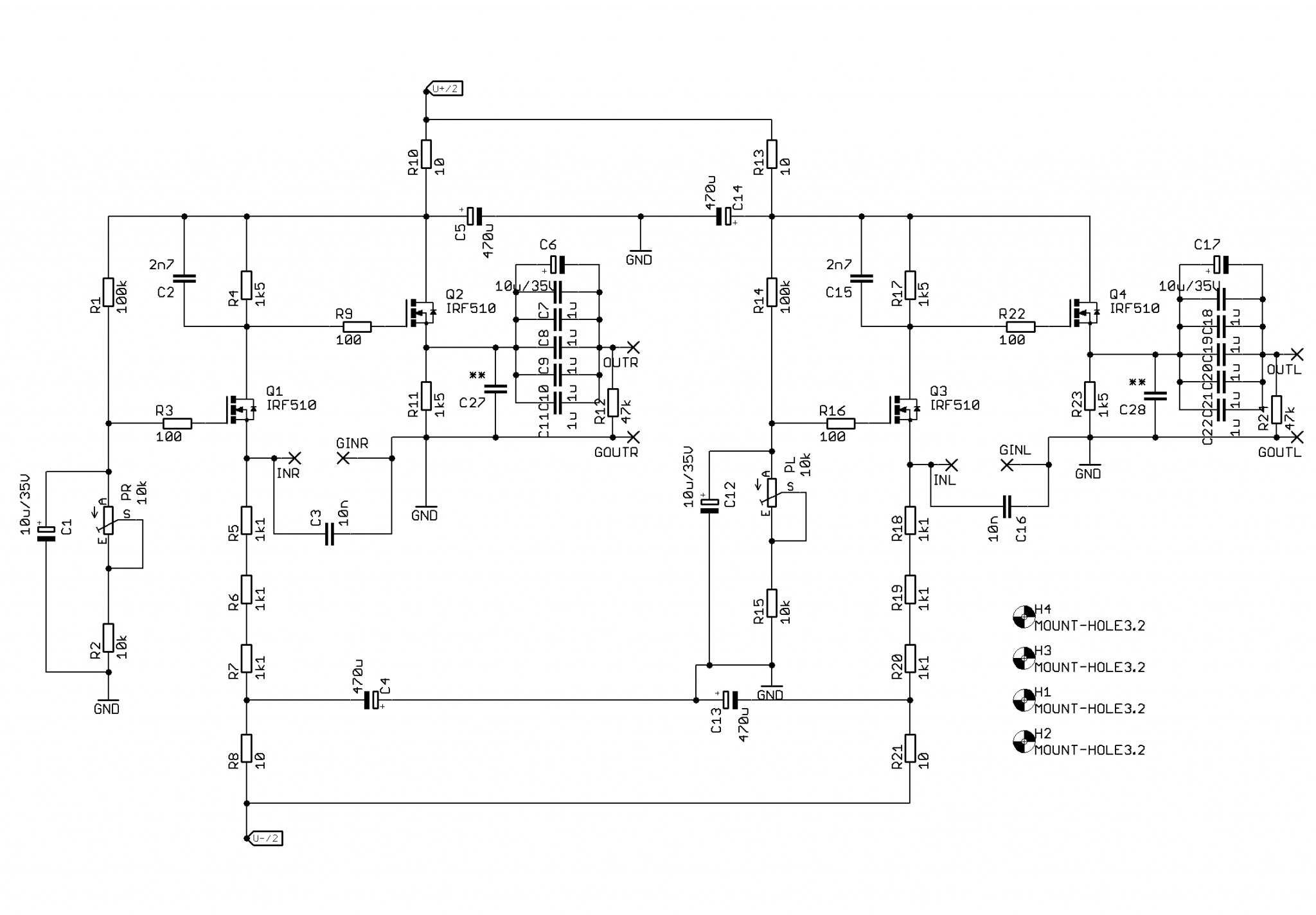
From my practice the best SQ (using any SUT) is possible ONLY using the i/v resistor across the primary coil. But the quality of this i/v resistor in the primary winding is DECISIVE for the sound quality, especially for the low-resistive resistors. And of course it is absolutely "possible/advisible with the transformers you have" 🖐I’m not knowledgeable enough to understand what affect having a resistor on the primary and secondary has on the performance of a passive i/v transformer…or if its even possible/advisable with the transformers I have.

Hello Zen Mod,
I would like to use the D1 I/V for two parallel TDA1541A.
Since I now have 2 x 4mA, i.e. 8mA output current, I would get 12Vpp or 4.2Veff.
( Uss = R4 x Idac Uss=1500R x 0.008A )
Is this still permissible for the D1 circuit or should adjustments be made to R4, C2, R11.
Should R4 be reduced to 750R here and can the value of C2 stay at 2.7nF?
Furthermore I only see ** with C27 but no value. What can you recommend here?
Thank you and regards
Richard
if you need to decrease gain of circuit, without ruining optimum DC points, best way is to assemble R4(R17) as two series connected resistors of 750R each
then connect nice elco cap, 1000uF/25V across upper one 750R resistor
that way 1K5 will still figure for steady state values, while in AC domain you'll have half gain, derived from 750R as dominating figure
C27 - use it or not, if you find sound of highest frequencies adequate, no need for that mild HP filter; it really depends most of everything preceding I/V stage itself
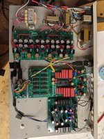
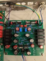
Hi All,
I recently built a TDA1541A DAC, using gerbers and info from the miro1360 thread; relevant info is at
https://www.diyaudio.com/community/...s-input-nos-r-2r.354078/page-268#post-7159210
The DAC sounds great; I've attached a photo - the output caps were a temporary safety measure while messing around with DC offset. Anyway, it sounds (or sounded) great. But of course I couldn't leave well enough alone, and my plan is to try other I/V ideas. Starting with the Pass D1, using the schematic two posts above this one, and ZM's gerbers posted elsewhere on the site - I forget where.
However the DC offset with the D1 is very bad (about 12V on both channels) so I've obviously done something wrong. Before I start searching for construction errors I'd like to ask whether I've disconnected and connected things incorrectly when changing I/V stages, since the TDA1541A supposedly has a big offset when you do that...
What I did on miro1360's board was to remove the opamps, lift R20 and R8 (and R22 and R9 from the other channel), and then connect pin 25 of the TDA1541A directly to INL on the circuit above. I thought that I would not need the DC offset circuitry on miro1360's board, since the D1 board has it. Is this right? Did I miss something else that has to disconnected? Or connected?
Thanks in advance for any help.
Attachments
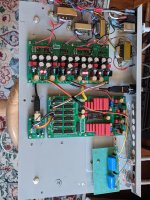
From your description it looks like you disconnected the existing output stage.
So there is something wrong with your D1 setup. A picture of the DAC with the D1 connected, showing all wiring and details of the D1 board would be very helpful. A picture of the previous setup without the D1 setup does not give any information on your current issue.
Did you connect the power supply ground to the D1 board?
With capacitors in the output of the D1 there should not be any DC offset.
Hi Ben,
I'll post photos shortly. To clarify, I'm not measuring the offset at the RCAs, but across R11 and R23. If I understand correctly, the TDA1541 has a 2mA offset that the trimpot on miro1360's board handles; I thought the arrangement on the D1 did the same thing? Either way, that's what I was measuring. I can check the RCAs but you're right - I'm sure there's no offset there.
The power supply board has separate grounds for each regulator (each of which has its own transformer). These are all connected together on the DAC board; the ground from the D1 board is also connected there - at least, it should be; I will check.
Have I misunderstood something about the 2mA offset business?
Last edited:
first test d1 pcb alone, to check are you able to set voltage level on input node
if that is OK (0V), check TDA output node voltage temporary shunted with 22R or something to gnd - it must be so-so 0V
then connect D1 to TDA (both gnd and input ) ; if both above are OK, you'll be able to set TDA out/D1 input to 0V, meaning that TDA is getting "missing" 2mA from D1 (input) current string
The 12V across R11 and R23 is a voltage of the D1 circuit. Disconnect the TDA from the D1 and it should still be there.
By the way, did you adjust the pot on each D1 channel to zero the voltage at the source of Q1 and Q3?
By the way, did you adjust the pot on each D1 channel to zero the voltage at the source of Q1 and Q3?
OK, Here are some photos. I had disconnected the D1 to measure some stuff, but it's all back as it was when I was measuring.
I checked ground connectivity; the center tap on the transformer for the D1 is connected to ground on the DAC board, and hence to the center tap on the other transformer.
I checked ground connectivity; the center tap on the transformer for the D1 is connected to ground on the DAC board, and hence to the center tap on the other transformer.
Attachments

The 12V across R11 and R23 is a voltage of the D1 circuit. Disconnect the TDA from the D1 and it should still be there.
Yes, it is. So I'm worried about nothing here? Was I measuring the wrong thing to see whether the 2mA was dealt with? Is this unimportant with the D1?
By the way, did you adjust the pot on each D1 channel to zero the voltage at the source of Q1 and Q3?
Aha! No, I didn't. Let me get on that...
first test d1 pcb alone, to check are you able to set voltage level on input node
Checked; yes, I can get it to 0. Or at least very near. (I didn't wait for it to warm up)
if that is OK (0V), check TDA output node voltage temporary shunted with 22R or something to gnd - it must be so-so 0V
Also 0V.
then connect D1 to TDA (both gnd and input ) ; if both above are OK, you'll be able to set TDA out/D1 input to 0V, meaning that TDA is getting "missing" 2mA from D1 (input) current string
Yes! This works fine; at least, I can get it to within 1mV, and I've left the unit to warm up and will adjust again.
Many thanks for the help. So the real problem was my lack of understanding of what the circuit is doing. As usual... I'll try the unit out once I've rechecked the offset, and will report back.
Best
Nigel


- Home
- Amplifiers
- Pass Labs
- NOS TDA1541 + D1 I/V & output stage