Hi,
What is the necessary setup and equations for tracing these noise figure plots?

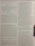
Plot from 2SC3324 datasheet.
What is the necessary setup and equations for tracing these noise figure plots?
Plot from 2SC3324 datasheet.
Last edited:
If these plots describe a device intrinsically, why it would depend on topology (for example, Common Emitter as it is described)?
Assuming small signal case, don't we always have available the one and the same transistor physics?
Assuming small signal case, don't we always have available the one and the same transistor physics?
Last edited:
is obsolete now, to be replaced by https://www.mouser.de/ProductDetail/Toshiba/2SC2713-BLLF?qs=R26iFe/kX/KGRY873m871g==
sorry plot is allegedly reported for 2SC3324
I want to trace the NF plots myself when they are not given.
this is not the point of the thread. 2SC3324 is just a /rare/ example with these NF plots published.is obsolete now
I want to trace the NF plots myself when they are not given.
Nevertheless, thank you for the link to the replacement!to be replaced by
Topic is how to make these measurements ourselves.
The noise plots are derivable from the voltage noise density and current noise density. Current noise is usually closely related to base current, voltage noise density is related to base-spreading resistance. However the flicker noise (1/f noise) behaviour is not so easily derived as it depends on transistor defect density among other things.
Once you have a voltage noise density and current noise density (for some operating point) their ratio will define the optimal source-impedance in that configuration [ where voltage noise matches input current noise reflected back from the source impedance, ie en/in = |Zsource| ]
The input-refered noise of a transistor is composed of three components which are usually treated as uncorrelated (for simplicity, reality is more complicated).
Rsource. provides Johnson noise of density = sqrt(4kTR) - the resistive part of source impedance contributes this
en, the input voltage noise of the device
in * |Zsource|, the input current noise reflects back from the source impedance as a voltage noise).
So total input-refered voltage noise density = sqrt (en^2 + (en * |Zsource|)^2 + 4kT * Rsource)
And total noise is that times the square root of the bandwidth.
in is typically about sqrt(2 * Ib * q). where q is the unit charge in coulombs (1.6e-19), Ib the base current in amps
So a transistor with 1µA base current, in would be about 0.55pA/√Hz
If it has 1nV/√Hz voltage noise, and the source is 1k + 2H (ie very inductive),
then the noise contributions at 1kHz are:
4nV/√Hz from Rsource
0.55pA * 2 * 1000 * 2pi. = 0.55pA * 12.5k = 7nV/√Hz from current noise into 2 henries (the source resistance is insignificant compared to the source inductance at 1kHz)
1nV/√Hz. (voltage noise).
sqrt (4*4 + 7*7 + 1*1) ~= 8,
so total noise 8nV/√Hz around 1kHz, with current noise dominating.

Hi Mark, okay, I got it. How do we get to these curves: setup + equations.
Tell me more please.
Btw, is there a 101 EE book (or an application Note of somebody, or even your own setup¬es) that teaches BJT noise and only noise? In all situations and how to measure it.
Or, at least the example above.
Tell me more please.
Btw, is there a 101 EE book (or an application Note of somebody, or even your own setup¬es) that teaches BJT noise and only noise? In all situations and how to measure it.
Or, at least the example above.
I think mark wrote the essentials about bjt noise. Looking at the plots you will find noise figure dependent from Rgen, IC and the D.U.T.
It is obvious that varying these 2 parameters independently with a single D.U.T requires a sophisticated laboratory setup.
So I recommend to narrow your parameter set to one or two values of Rgen and a collector current to a fixed value
in the ballpark of 100uA that makes comparision between different D.U.T.s doable.
ideally, what means noise matching? why is it important? Why not mismatch (NF=0 is a mismatch, right)?
It may be so, but let's be positive here. Topic is not limited to simple setups, but to the 'correct setup'.requires a sophisticated laboratory setup.
If not for educational value, at least for fun.
I suppose noise matching means designing the circuitry in a way that the noise of the very first stage dominates resulting output noise.
All in all this is the solution for smallest noise referred to the input.
All in all this is the solution for smallest noise referred to the input.
I am quite sure there exist(ed) apparatus to do this job. Never met such thing but I am sure the innards are beyond DIY entry level.It may be so, but let's be positive here. Topic is not limited to simple setups, but to the 'correct setup'.
If not for educational value, at least for fun.
There is a German guy living in Canada who is "the noise pope". You may find him here or on mikrocontroller.net. His name is Gerhard O.
I am quite sure there exist(ed) apparatus to do this job. Never met such thing but I am sure the innards are beyond DIY entry level.
In contrary, transistor noise is easy to measure. You need this circuit from ArtOfElectronics3 and
a spectrum analyzer. That could be a sound card. You do not even need to know the exact gain /
sensitivity of your sound card. And a large metal cookie box helps, too.
Gerhard H
I don't even know which street canaduh is on! (Al Capone)
Attachments
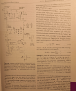
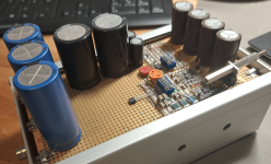
I like the ground in mybuild 🙂
The Horrowitz&Hill and especially the special cookie box can be sourced. The contents of the box can be traded for the digital form of H&H.
Again, if the ideal case we want is NF=0 then why we call it noise matching? Which are the physical parameters to match?
The Horrowitz&Hill and especially the special cookie box can be sourced. The contents of the box can be traded for the digital form of H&H.
Again, if the ideal case we want is NF=0 then why we call it noise matching? Which are the physical parameters to match?
Gerhard_H (not _O)
I actually suspected it was you the best candidate for noise pope 🙂
Or cardinal. Whichever title you feel comfortable with.
Thanks for the pages!
Can you help here with clarifications of terminology vs practical & theory?
I actually suspected it was you the best candidate for noise pope 🙂
Or cardinal. Whichever title you feel comfortable with.
Thanks for the pages!
Can you help here with clarifications of terminology vs practical & theory?
okayRsource. provides Johnson noise of density = sqrt(4kTR) - the resistive part of source impedance contributes this
en, the input voltage noise of the device
why |Zsource|? I need to see more into its derivation work to understand it.in * |Zsource|, the input current noise reflects back from the source impedance as a voltage noise).
'reflects back': you mean 'creates'?
Thanks! I need time to try to digest it a bit more.I think mark wrote the essentials about bjt noise. Looking at the plots you will find noise figure dependent from Rgen, IC and the D.U.T.
It is obvious that varying these 2 parameters independently with a single D.U.T requires a sophisticated laboratory setup.
So I recommend to narrow your parameter set to one or two values of Rgen and a collector current to a fixed value
in the ballpark of 100uA that makes comparision between different D.U.T.s doable.
Actually I do not understand. Why the NF traces are stopping at 1dB and 12dB?
The traces of 0.1dB and 0.01dB will overlap? Still... why not show them?
The traces >12dB not interesting?
Last edited:
Here’s my layman’s explanation 🙂
Even with a 0-ohm source resistance, the device has it’s inherent self noise which is all voltage noise. Noise voltage is always there, but as you add source resistance the total noise goes up due to the thermal noise of the resistor and the current noise due to base current flowing in the source resistance.
The curves plot out the best/worst noise performance of the collector op. current vs source resistance in your circuit.
- Home
- Amplifiers
- Solid State
- Noise plots tracing for transistors