OK. I did it with CircuitMaker. I think you use LTSpice, so I will make one with that software and post it soon.Post your simulation, I still do not understand what you did...
Regards - Godfrey
Nice result, Keantoken.
Hey, wait, you cheated - Q7/Q8 is a cfp - that counts as multi-stage feedback!
Seriously, though - Although this is only an academic exercise, I think it's really valuable because it gets one thinking about how to maximize open-loop performance.
I really don't subscribe to the "make any mess and fix it with feedback" school of design.
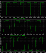
You really get to appreciate this kind of design when you look at the distortion at 100kHz or 1MHz and see it's not much worse than at 1kHz.
Contrast that with, for example, Edward Cherry's NDFL design where sensitive viewers are best advised not to ask what happens above 20kHz.
Cheers - Godfrey
Hey, wait, you cheated - Q7/Q8 is a cfp - that counts as multi-stage feedback!
Seriously, though - Although this is only an academic exercise, I think it's really valuable because it gets one thinking about how to maximize open-loop performance.
I really don't subscribe to the "make any mess and fix it with feedback" school of design.
You really get to appreciate this kind of design when you look at the distortion at 100kHz or 1MHz and see it's not much worse than at 1kHz.
Contrast that with, for example, Edward Cherry's NDFL design where sensitive viewers are best advised not to ask what happens above 20kHz.
Cheers - Godfrey
I agree, Godfrey. A no-NFB design exercise teaches us how to treat nonlinear devices in sub-optimal conditions. If you look at Tektronix scope schematics from the 60's, you notice the lack of NFB and the simplicity of circuitry used.
Yes, the circuit does have some internal NFB, only in the output stage... The CFP could be described as a Gm-divider. It divides the Gm of the master device using the slave to offload the current. This decreases output impedance and divides output error.
Using feedback as a "catch-all" measure and neglecting close scrutiny of the internals is not conducive to developing good engineering skill. I'm thinking maybe there should be a no-NFB forum where we all pursue open-loop design not necessarily in a practical sense, but as an intellectual exercise to improve our design skills in feedback designs? The idea is there anyways.
- keantoken
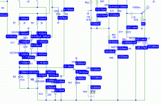

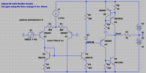
For no feedback, I recommend at least another EF stage in the output stage, turning it into a triple EF. As it is, output transistor base currents will cause lots of error at the final VAS stage (R64 and R70).
Also, the complementary VAS's Q42 and its compliment; these transistors have diode transfer curves and so even if I(R33) and I(R25) are linear, the transistors' transfer curves will add to produce a big bulge of a transfer curve.
To remedy this I recommend that you turn Q42 and its compliment into a current mirror arrangement like I have in my schematic. This will linearize the final VAS and give it a linear transfer curve, reducing distortion. As it is, the Vbe of Q42 is not compensated for and will cause much error.
Emitter resistors in the current mirrors can be varied to give some amplification of their own, but this disrupts matching and canceling of Vbe's and I have found this to actually be the largest source of distortion in the no-feedback circuits I have simulated. Whenever it produced more distortion than I liked, it was always when I modified a current mirror ratio. So I suggest for no-feedback design that current mirrors be left as current mirrors and for gain to be added in other stages.
- keantoken
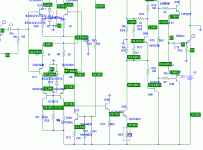
I did try an amp with no GNFB , and as proposed by Havenwood; i did choose
a symetrical differential which seems more adequate than a single differential.
Anyway, distorsion figures are quite high, in the 0.2% range.
a symetrical differential which seems more adequate than a single differential.
Anyway, distorsion figures are quite high, in the 0.2% range.
😕Anyway, distorsion figures are quite high, in the 0.2% range.
high???
your speaker gives ~1%
😱
anything bellow 10%
is realy good

😕
high???
your speaker gives ~1%
😱
anything bellow 10%
is realy good
Padamiecki, you are right.
I suppose that we are all influenced by the 0.0000000X figures
we see here and there, so we lost contact with reality about
audible distorsions thresholds..
By the way, greetings to Krakow, as my girl friend family originate
from this town.
The psychology of numerical appraisal......
Well known phenomenon originally noted in the 1920s.
Hugh
Well known phenomenon originally noted in the 1920s.
Hugh
The psychology of numerical appraisal......
Well known phenomenon originally noted in the 1920s.
Hugh
hi, hugh..
yes, psychologicaly, they sound better !!!
Thanks to All for posting their circuits
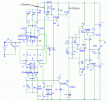
For example: Doing some simulations, found that the decrease in gain circuit without NFB to increase the bandwidth, reduces distortion. Perhaps that explains why an amp would be better with low negative feedback and more bandwidth in Open-Loop, but this with circuit no feedback (attached).
A circuit with global feedback things are different, decrease in gain Open-Loop does not decrease the distortion.
Another thing we must realize, I'm using is Base Stoppers this reduces the distortion. I realized this in circuit D.Self (Blameless).
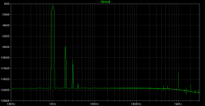
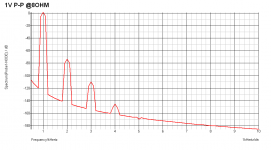
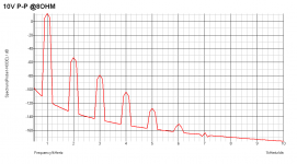
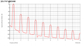
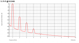
TDH 20Khz = 0.014112%
4V RMS - 300R
The idea is to make a circuit low distortion, from a certain point not need NFB. If a circuit is better or worse with NFB I do not know. I think not, but nothing prevents you from studying circuits without NFB.I agree, Godfrey. A no-NFB design exercise teaches us how to treat nonlinear devices in sub-optimal conditions. If you look at Tektronix scope schematics from the 60's, you notice the lack of NFB and the simplicity of circuitry used.
Using feedback as a "catch-all" measure and neglecting close scrutiny of the internals is not conducive to developing good engineering skill. I'm thinking maybe there should be a no-NFB forum where we all pursue open-loop design not necessarily in a practical sense, but as an intellectual exercise to improve our design skills in feedback designs? The idea is there anyways.
For example: Doing some simulations, found that the decrease in gain circuit without NFB to increase the bandwidth, reduces distortion. Perhaps that explains why an amp would be better with low negative feedback and more bandwidth in Open-Loop, but this with circuit no feedback (attached).
A circuit with global feedback things are different, decrease in gain Open-Loop does not decrease the distortion.
Another thing we must realize, I'm using is Base Stoppers this reduces the distortion. I realized this in circuit D.Self (Blameless).
TDH 20Khz = 0.014112%
4V RMS - 300R
Attachments
Last edited:
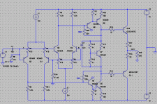
What about this amp:
No global NFB, Gain ~20, THD@20kHz 0.25%, Iq=240mA.
Full simetry cascode input.
Maybe Sziklai output stage?
From my little experience, output EF in class A not is good, Sziklai is better in class A.
[snip]A circuit with global feedback things are different, decrease in gain Open-Loop does not decrease the distortion.
[snip]
Depends. When you go from open loop to feedback (with the same amp) the distortion reduction and bandwidth increase is in ratio with the gain reduction.
Example: open loop gain = 1000, now use feedback to make gain 20, is reduction by 50. Your distortion is now reduced 50x and the bandwidth is 50x greater.
In this situation, if you now make the ol gain 200 instead of 1000, of course your distortion in principle rises 5x and the bandwidth gets 5x smaller.
BUT if you bring the ol gain from 1000 to 200 by for instance using local feedback in some amp stages, that local fb can lower the distortion in the amp so you may not see the 5x distortion increase.
jd
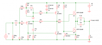
Something else you got right there is inherently good Power Supply Rejection.How does this look? Still no GNFB from output.
Looking back on the last few posted circuits ito PSRR:
Havenwood's circuit addresses the issue by referencing the output voltage to ground with R64 and R70. (Mine did the same with R8).
Keantoken's circuit fail's in this respect by referencing the output to the positive rail with R6. Similarly, Rafael's circuit references both supply rails with the feedback resistors around the VAS stages.
Ah well, there it is - something else to think about besides THD.
🙂
btw, Shaan: what software are you using?
My copy of CircuitMaker "student edition" has a couple of ugly bugs and I find LtSpice a real pain to use...
Last edited:
- Status
- Not open for further replies.
- Home
- Amplifiers
- Solid State
- No feedback amp