Because of no loop gain the voltage across the LTP inputs is almost a volt instead of the usual 10s of mv so to keep them linear?
Yes, they pull a very high diff input voltage. This is always a problem on a LTP because of diff Vbe set up across the two opposing devices, leading to lots of symmetrical (odd order) distortion.
I'm sure this is a lovely amp, but I'd really like to hear one......
Hugh
I'm sure this is a lovely amp, but I'd really like to hear one......
Hugh
Yes I agree with you Bob. Feedback is indeed a friend -I was just providing some pointers.
The proposal to use a diamond buffer elsewhere is a good one if this amplifer is being used for preamp duties.
The proposal to use a diamond buffer elsewhere is a good one if this amplifer is being used for preamp duties.
You must be referring to R7 is a shunt VAS.Try this one!
THD 1.19% at 1KHz, +20dB, Av of just below 50, zero global feedback, no compensation, stable. It clips early on the negative half cycle around -29V due to the heavy VAS degeneration.
This circuit still uses the feedback output of the VAS. Is actually, the output stage is outside the feedback, therefore low damping factor.
I made more two simulations.
Fig 1
inverting amplifier (no differentiator)
DC component:-0.000769105
Harmonic Frequency Fourier Normalized Phase Normalized
Number [Hz] Component Component [degree] Phase [deg]
1 2.000e+04 4.999e+00 1.000e+00 178.46° 0.00°
2 4.000e+04 3.241e-05 6.483e-06 178.43° -0.03°
3 6.000e+04 4.251e-06 8.504e-07 -81.49° -259.94°
4 8.000e+04 6.206e-07 1.242e-07 -10.77° -189.22°
5 1.000e+05 1.184e-07 2.368e-08 98.46° -80.00°
6 1.200e+05 1.873e-08 3.746e-09 172.05° -6.41°
7 1.400e+05 1.127e-08 2.255e-09 -172.90° -351.36°
8 1.600e+05 8.393e-10 1.679e-10 71.31° -107.15°
9 1.800e+05 1.450e-08 2.900e-09 -18.17° -196.63°
Total Harmonic Distortion: 0.000654%
Fig 2 Decreased feedback (30dB loop Gain)
Harmonic Frequency Fourier Normalized Phase Normalized
Number [Hz] Component Component [degree] Phase [deg]
1 2.000e+04 5.328e+00 1.000e+00 -0.97° 0.00°
2 4.000e+04 7.191e-05 1.350e-05 157.17° 158.14°
3 6.000e+04 5.347e-06 1.004e-06 88.94° 89.91°
4 8.000e+04 2.274e-08 4.268e-09 139.44° 140.41°
5 1.000e+05 3.089e-08 5.797e-09 -159.97° -159.00°
6 1.200e+05 3.596e-08 6.750e-09 -178.90° -177.93°
7 1.400e+05 1.248e-08 2.342e-09 -133.81° -132.84°
8 1.600e+05 2.191e-08 4.113e-09 -171.43° -170.46°
9 1.800e+05 3.392e-08 6.367e-09 165.98° 166.94°
Total Harmonic Distortion: 0.001353%
Attachments
Negative feedback is your friend.
Cheers,
Bob
Hi Bob
is only for testing and simulations, remembering that you also already made 🙄
http://www.cordellaudio.com/papers/phase_intermodulation_distortion.pdf
You must be referring to R7 is a shunt VAS.
Indeed, the VAS gives the primary voltage gain, so it is fixed resistively since feedback is not used.
This circuit still uses the feedback output of the VAS.
You are referring to my schematic? If so, wrong. It is used in DC only, since all AC is shunt directly to ground by the large cap from the inverting mode. You must use DC feedback, NOT AC, to achieve offset control, no small issue in a direct coupled amp.
Is actually, the output stage is outside the feedback, therefore low damping factor.
But of course. If you want high DF, you MUST use negative feedback, there is no other way!
You cannot have it both ways......
The exercise is educational, but not practical. Good luck in your quest.
Last edited:
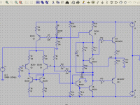
Hi all
With no global feedback, the VAS should have well defined current gain and load impedance. Something like the attached circuit could be good.
Features:
Balanced or unbalanced input
Class A output to about +-20mA
Reasonable thermal stability and PSRR
Good HF stability
Zero global or multistage feedback
No electrolytics
Voltage gain: about 40
Zin: about 10K
Zout: <50R
LF rolloff: about 7Hz
HF rolloffs: about 300KHz @ input, 600KHz @ VAS
Distortion: ???
The transistors shown are just random jellybeans, not recommended devices.
FWIW here's what my sim thinks:
100mV RMS in @ 1Khz => 3.5V RMS out
2'nd harmonic about 0.2%
3'rd harmonic about 0.01%
all others 0.001% or lower
100mV RMS in @ 100Khz => 3.0V RMS out
2'nd harmonic about 0.5%
3'rd harmonic about 0.1%
all others 0.002% or lower
Hmm... not a bad start, distortion needs some work though.
It's something to play with, anyway. 🙂
Cheers - Godfrey
Attachments
Last edited:
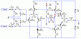
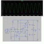
No feedeback amp
I did a double pair symmetric only testing (not optimized)
Gain 64dB
DC component:-0.00727194
Harmonic Frequency Fourier Normalized Phase Normalized
Number [Hz] Component Component [degree] Phase [deg]
1 2.000e+04 5.053e+00 1.000e+00 -49.51° 0.00°
2 4.000e+04 1.656e-03 3.277e-04 -100.76° -51.24°
3 6.000e+04 3.906e-03 7.730e-04 -136.31° -86.80°
4 8.000e+04 2.788e-05 5.518e-06 94.76° 144.27°
5 1.000e+05 5.288e-05 1.046e-05 -59.20° -9.68°
6 1.200e+05 9.266e-07 1.834e-07 165.85° 215.36°
7 1.400e+05 1.053e-06 2.085e-07 18.09° 67.60°
8 1.600e+05 4.502e-08 8.909e-09 -150.68° -101.16°
9 1.800e+05 5.009e-08 9.913e-09 125.68° 175.19°
Total Harmonic Distortion: 0.083965%
Attachments
Hi all
With no global feedback, the VAS should have well defined current gain and load impedance. Something like the attached circuit could be good.
Features:
Balanced or unbalanced input
Class A output to about +-20mA
Reasonable thermal stability and PSRR
Good HF stability
Zero global or multistage feedback
No electrolytics
Voltage gain: about 40
Zin: about 10K
Zout: <50R
LF rolloff: about 7Hz
HF rolloffs: about 300KHz @ input, 600KHz @ VAS
Distortion: ???
The transistors shown are just random jellybeans, not recommended devices.
FWIW here's what my sim thinks:
100mV RMS in @ 1Khz => 3.5V RMS out
2'nd harmonic about 0.2%
3'rd harmonic about 0.01%
all others 0.001% or lower
100mV RMS in @ 100Khz => 3.0V RMS out
2'nd harmonic about 0.5%
3'rd harmonic about 0.1%
all others 0.002% or lower
Hmm... not a bad start, distortion needs some work though.
It's something to play with, anyway. 🙂
Cheers - Godfrey
You have sure that this circuit works without feedback?
I think that is a discrete opamp
Yes, try it! 🙂You have sure that this circuit works without feedback?
The voltage gain stage has low current gain, about 10, same as your last circuit, but the transconductance of the input stage is much lower.
Also: the gain is low because the voltage gain stage drives a low load impedance (R6 in my circuit). Opamps always try to get high gain by making the load impedance as high as possible.
R6 keeps the gain down and also makes it easier to set the DC offset.
Cheers - Godfrey
Member
Joined 2009
Paid Member
But of course. If you want high DF, you MUST use negative feedback, there is no other way!
I may be showing my inexperience again, but I've read somewhere where the tube guys used multiple tubes to lower output impedance and hence improve DF without feedback. Perhaps the improvement is not very much and multiple output devices would never get into 'high' DF territory ?????
Yes, try it! 🙂
The voltage gain stage has low current gain, about 10, same as your last circuit, but the transconductance of the input stage is much lower.
Also: the gain is low because the voltage gain stage drives a low load impedance (R6 in my circuit). Opamps always try to get high gain by making the load impedance as high as possible.
R6 keeps the gain down and also makes it easier to set the DC offset.
Cheers - Godfrey
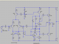
But the topology simple differential pair, you need to compensate the DC of the VAS NPN, that makes such compensation is the transistor PNP in input pair.
Where is connecting the inverting input?
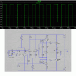
Small optimizations
Gain 28.8dB
THD 20 KHz 4V RMS
DC component:-0.0029007
Harmonic Frequency Fourier Normalized Phase Normalized
Number [Hz] Component Component [degree] Phase [deg]
1 2.000e+04 5.527e+00 1.000e+00 -3.45° 0.00°
2 4.000e+04 8.850e-04 1.601e-04 81.51° 84.96°
3 6.000e+04 1.375e-03 2.489e-04 53.49° 56.94°
4 8.000e+04 3.024e-05 5.471e-06 -29.22° -25.77°
5 1.000e+05 5.409e-05 9.786e-06 -125.78° -122.33°
6 1.200e+05 2.587e-06 4.680e-07 138.08° 141.53°
7 1.400e+05 2.941e-06 5.321e-07 39.90° 43.35°
8 1.600e+05 1.912e-07 3.459e-08 -58.83° -55.38°
9 1.800e+05 1.892e-07 3.423e-08 -154.67° -151.22°
Total Harmonic Distortion: 0.029613%
Square Wave no symmetric
Attachments
Last edited:

Hi Gareth,
Yes, multiple tubes will reduce Zout, BUT, the classic case, the OTL, where no output transformer is used, also uses lashes of feedback.
In the case of emitter follower bipolar stages, you can reduce Zout by increasing the pairs, certainly, but you are always somewhat limited. It depends what you want; if you want a DF of 400, a common goal for a large amp, you would need perhaps eight output pairs, but for more moderate demands, say 40, a couple of output pairs would do the job. But you always have the signal compression from an unmoderated output stage, that is, one whose error is not ameliorated with negative feedback.
Good circuit, Rafael! Like the way you control offset.....
But there's no free lunch.
Hugh
Nice!Small optimizations
Now you have feedback around the VAS to control the gain and DC offset.
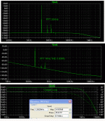
😕Square Wave no symmetric
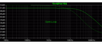
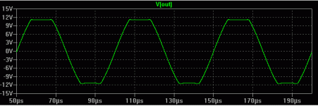
If you use a sine wave and make it slowly bigger, bigger, bigger then you can see what happens.
I think it will start to look like this picture.
After that, I don't know...
Attachments

Last edited:
Don´t forget that there is quite heavy local current feedback in the input diff stages in the later shown schematics. This can be one of the reasons they sim good. Haven´t read the whole thread so this might have been mentioned before.
Nice!
Now you have feedback around the VAS to control the gain and DC offset.
😕
If you use a sine wave and make it slowly bigger, bigger, bigger then you can see what happens.
I think it will start to look like this picture.
After that, I don't know...
Is that there is an asymmetry with a difference of 1V. But was due to removal of the capacitor I was confused, clipping is symmetry.
BTW
Post your simulation, I still do not understand what you did...
Attachments
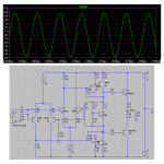
More optimizations, the circuit does not use compensating
DC component:-0.00196752
Harmonic Frequency Fourier Normalized Phase Normalized
Number [Hz] Component Component [degree] Phase [deg]
1 2.000e+04 5.711e+00 1.000e+00 -1.05° 0.00°
2 4.000e+04 5.181e-04 9.072e-05 -13.49° -12.44°
3 6.000e+04 8.590e-04 1.504e-04 52.23° 53.28°
4 8.000e+04 1.036e-05 1.813e-06 159.00° 160.05°
5 1.000e+05 2.154e-05 3.772e-06 -103.14° -102.08°
6 1.200e+05 1.067e-07 1.868e-08 -60.17° -59.12°
7 1.400e+05 8.676e-07 1.519e-07 74.28° 75.33°
8 1.600e+05 3.846e-09 6.734e-10 59.67° 60.73°
9 1.800e+05 4.385e-08 7.677e-09 -107.56° -106.51°
Total Harmonic Distortion: 0.017569%
Attachments
- Status
- Not open for further replies.
- Home
- Amplifiers
- Solid State
- No feedback amp