Something else you got right there is inherently good Power Supply Rejection.
Looking back on the last few posted circuits ito PSRR:
Havenwood's circuit addresses the issue by referencing the output voltage to ground with R64 and R70. (Mine did the same with R8).
Keantoken's circuit fail's in this respect by referencing the output to the positive rail with R6. Similarly, Rafael's circuit references both supply rails with the feedback resistors around the VAS stages.
Ah well, there it is - something else to think about besides THD.
🙂
btw, Shaan: what software are you using?
My copy of CircuitMaker "student edition" has a couple of ugly bugs and I find LtSpice a real pain to use...
You pointed it right. It does show better hum removal with simple supplies. Plus is sounds so sweet.
 🙂
🙂It is Simetrix V5.5 I am using. Demo. But can be used indefinitely.
For a newbie like me it is really an easy-to-use app.
Link-> simetrix dot co dot uk/cgi-bin/download1.pl?id=168021
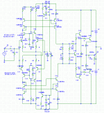
Hi, how is the transfer function of current mirror like the circuit?Also, the complementary VAS's Q42 and its compliment; these transistors have diode transfer curves and so even if I(R33) and I(R25) are linear, the transistors' transfer curves will add to produce a big bulge of a transfer curve.
A linear transfer vs exp(Vbe/Vt)?
I try with this circuit concept (attachments)
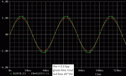
Vin=0.1V, Gain ~18, THD@1kHz 0.163%, Iq=165,54mA
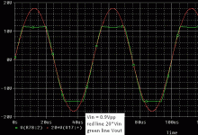
With Vin=0.9Vpp, Vout=10Vpp
Gain ~10 and THD 10% V(3rd harmonic 1V 🙄 )
This is because I use cascode input? What is de Vce optimal for cascode (low power amplifier >25W)?
Attachments

Last edited:
The current gain of your output transistors is low and very non-linear at high currents. With high output power, their base currents will be large and badly distorted.With Vin=0.9Vpp, Vout=10Vpp
Gain ~10 and THD 10% V(3rd harmonic 1V 🙄 )
It looks like you have 47R resistors in series with their bases. The voltage drop across these will cause distortion and loss of output voltage.
Try taking out these resistors. It should help a lot.
Cheers - Godfrey
p.s. @Shaan: Thanks! I'll give Simetrix a try.
Last edited:
Simetrix..
I use it as well, and it s a good simulator, not counting the neat schematics....
Nice!
Do you use the intro version?
Havenwood, I am not sure why the THD jumped like that. A tip for setting the output bias: probe between Q45's base and the output and adjust bias until the waveform is a pure sinewave.
Go back to your previous schematic and check for differences between the two, such as:
Bias current of Q44 and Q43
Bias current of output stage
Output and input levels where THD was measured, and gain (these all affect THD levels proportionately, so you must take this into account when measuring)
- keantoken
The current gain of your output transistors is low and very non-linear at high currents. With high output power, their base currents will be large and badly distorted.
It looks like you have 47R resistors in series with their bases. The voltage drop across these will cause distortion and loss of output voltage.
Try taking out these resistors. It should help a lot.
Cheers - Godfrey
p.s. @Shaan: Thanks! I'll give Simetrix a try.
Yes, at high output currents base current demands for the output devices could easlily be 1 amp. With 47 ohms at those bases, yoiu would need 47V between emitter of driver and base of output device for that. Clearly, that's not going to fly...
jd
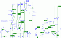
Why this clipping?
Hi Havenwood,
just put the probe marker at the colloctor of Q23
and mark transients plot😉
Also look at the voltage drop across R67 and R68 😉Why this clipping?
- Status
- Not open for further replies.
- Home
- Amplifiers
- Solid State
- No feedback amp