I've come up with a possible new topology for the input stage and VAS of an amplifier using opamps well above their normal voltage limits.
Background:
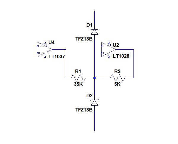
A negative impedance converter (NIC) is an opamp circuit that synthesizes a negative input impedance. In the diagram point A is the where the negative impedance is created.


the input impedance formula is: - R1 * R3 / R2
Here that's - 15k x 10k / 5k = -30k
So I add +30k as R4 to this, creating zero impedance at input - or put another way a current-mode input. With this circuit each milliamp of current at the input gives 40V at the output, and the opamp magically keeps the input at virtual ground.
Note that the opamp inputs are at 30V when the output is hypothetically at 40V - in other words if we can bootstrap or float the opamp supply suitably this circuit only sees a differential of 10V across its terminals for each mA of input current.
Given a real opamp capable of running at +/- 18V, and able to drive to within 3V of each rail, we have 30V of voltage differential available, so this circuit with 3mA input would see point A at 90V and the output at 120V (and similarly for negative swings).
I split R3 into two equal parts to provide a bootstrap voltage that's midpoint between the inputs and output of the opamp, and use zeners and BJTs to bootstrap the supply so it can swing up and down with the signal.


The left hand opamp does the input and loop feedback, the right hand one is the NIC.
Note that the bootstrapping takes a small amount of current from the network, distorting the behaviour slightly. However the first opamp closes a feedback loop around the whole circuit (its the input stage in effect) which re-linearizes this. Driving the current into the negative impedance converter effectively boosts the open loop gain as this integrates the input opamp's voltage signal.
I fiddled around with compensation in an ad-hoc manner, to get the simulation stable and not too horrid on clipping or square waves, but there's lots more fun to be had working on compensation on a breadboarded version I think 🙂
The ratio R1+R2 : R2 sets the voltage swing magnification factor of the circuit. This can be tailored to the voltage rails - here 120V = 4 x 30V (where 30V is my opamp signal swing range), so I've used a ratio of 4, ie R1 = 3 * R2.
I've added rudimentary diode input and output protection to the opamp stages, and the high value of the inter-stage resistor allows this to limit currents to safe levels - again experimentation with a breadboarded circuit as to the robustness of the scheme is needed.
The output stage and biasing arrangements are just lashed up as a demo for simulation - for instance voltage limits and secondary breakdown limits are no doubt completely exceeded and there's no thermal compensation! I'm not so interested in comments about these parts of the circuit 🙂
But comments on the idea are very welcome!
[PS Some of the images from posts below seem to have vanished recently, I'll include them here:
NIC_plot.png:

NIC_wave.png:

NIC_wave_detail.png:

NIC_scope.png:

Background:
A negative impedance converter (NIC) is an opamp circuit that synthesizes a negative input impedance. In the diagram point A is the where the negative impedance is created.
the input impedance formula is: - R1 * R3 / R2
Here that's - 15k x 10k / 5k = -30k
So I add +30k as R4 to this, creating zero impedance at input - or put another way a current-mode input. With this circuit each milliamp of current at the input gives 40V at the output, and the opamp magically keeps the input at virtual ground.
Note that the opamp inputs are at 30V when the output is hypothetically at 40V - in other words if we can bootstrap or float the opamp supply suitably this circuit only sees a differential of 10V across its terminals for each mA of input current.
Given a real opamp capable of running at +/- 18V, and able to drive to within 3V of each rail, we have 30V of voltage differential available, so this circuit with 3mA input would see point A at 90V and the output at 120V (and similarly for negative swings).
I split R3 into two equal parts to provide a bootstrap voltage that's midpoint between the inputs and output of the opamp, and use zeners and BJTs to bootstrap the supply so it can swing up and down with the signal.
The left hand opamp does the input and loop feedback, the right hand one is the NIC.
Note that the bootstrapping takes a small amount of current from the network, distorting the behaviour slightly. However the first opamp closes a feedback loop around the whole circuit (its the input stage in effect) which re-linearizes this. Driving the current into the negative impedance converter effectively boosts the open loop gain as this integrates the input opamp's voltage signal.
I fiddled around with compensation in an ad-hoc manner, to get the simulation stable and not too horrid on clipping or square waves, but there's lots more fun to be had working on compensation on a breadboarded version I think 🙂
The ratio R1+R2 : R2 sets the voltage swing magnification factor of the circuit. This can be tailored to the voltage rails - here 120V = 4 x 30V (where 30V is my opamp signal swing range), so I've used a ratio of 4, ie R1 = 3 * R2.
I've added rudimentary diode input and output protection to the opamp stages, and the high value of the inter-stage resistor allows this to limit currents to safe levels - again experimentation with a breadboarded circuit as to the robustness of the scheme is needed.
The output stage and biasing arrangements are just lashed up as a demo for simulation - for instance voltage limits and secondary breakdown limits are no doubt completely exceeded and there's no thermal compensation! I'm not so interested in comments about these parts of the circuit 🙂
But comments on the idea are very welcome!
[PS Some of the images from posts below seem to have vanished recently, I'll include them here:
NIC_plot.png:
NIC_wave.png:
NIC_wave_detail.png:
NIC_scope.png:
Last edited:


Code:
Fourier components of V(output)
DC component:6.00273e-06

Harmonic    Frequency     Fourier     Normalized     Phase      Normalized
 Number       [Hz]       Component     Component    [degree]    Phase [deg]
    1        1.000e+3     1.056e+2     1.000e+0        0.00°        0.00°
    2        2.000e+3     5.659e-5     5.359e-7       67.85°       67.85°
    3        3.000e+3     8.027e-4     7.601e-6       94.90°       94.90°
    4        4.000e+3     3.481e-5     3.297e-7      -13.89°      -13.89°
    5        5.000e+3     1.475e-4     1.397e-6      -60.26°      -60.26°
    6        6.000e+3     1.729e-4     1.637e-6      -14.92°      -14.92°
    7        7.000e+3     2.421e-4     2.292e-6       45.06°       45.06°
    8        8.000e+3     9.226e-5     8.737e-7      144.98°      144.98°
    9        9.000e+3     8.638e-5     8.180e-7      133.10°      133.10°
   10        1.000e+4     1.123e-4     1.063e-6      156.24°      156.24°
   11        1.100e+4     6.433e-5     6.091e-7      -88.14°      -88.14°
   12        1.200e+4     1.288e-4     1.219e-6      -13.53°      -13.53°
   13        1.300e+4     2.554e-4     2.418e-6      -28.29°      -28.29°
   14        1.400e+4     2.752e-5     2.606e-7      -25.09°      -25.09°
   15        1.500e+4     1.406e-4     1.331e-6      140.71°      140.71°
   16        1.600e+4     1.086e-4     1.028e-6       56.67°       56.67°
   17        1.700e+4     6.832e-5     6.469e-7      149.79°      149.79°
   18        1.800e+4     9.100e-5     8.617e-7      -90.75°      -90.75°
   19        1.900e+4     4.841e-5     4.585e-7     -112.57°     -112.57°
   20        2.000e+4     2.459e-4     2.329e-6      -37.44°      -37.44°
Total Harmonic Distortion: 0.000938%(0.000000%)
Cyan is the supposed virtual ground point, which isn't quite ground due to the bootstrap circuit's interference, but is well within the output range of the first opamp. Green and blue are point A and output of the NIC, magenta and grey are bootstrapped supply voltages for the NIC opamp.
Detail of the cyan plot:

One last thing, its DC coupled as the bootstrapping doesn't use capacitors, although you could swap current sources for a capacitive bootstrap if you wanted.
Last edited:
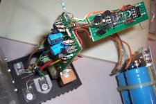
And it does actually work on a breadboard (at lowish voltages at least):

green: drive to the 30k resistor
blue: point A
magenta: opamp out
yellow: upper opamp bootstrapped rail. All 10V/div, 1kHz test tone.
This was with the same gain structure as my circuit above, gain of 48 set by 1k/47k resistors on the first opamp and resistances as in my description except 4k7 replaces 5k. The zeners are driven just from resistors rather than current sources, making the green trace even less like a virtual ground than in the sim.
Last edited:
What a delightful idea! Congratulations. I trust you won't be driving Apogee Scintillas (2 ohm ribbon loudspeakers) with a plus/minus 120V power supply and a single pair of output transistors.
Does it work in similar way as Elvee's circuit here?
(except for the current dumping of course)..
https://www.diyaudio.com/forums/solid-state/263065-ez-dump-dump-current-trying-8.html#post6054341
(except for the current dumping of course)..
https://www.diyaudio.com/forums/solid-state/263065-ez-dump-dump-current-trying-8.html#post6054341
Does it work in similar way as Elvee's circuit here?
(except for the current dumping of course)..
https://www.diyaudio.com/forums/solid-state/263065-ez-dump-dump-current-trying-8.html#post6054341
Ooh, yes, I've not figured out that circuit in detail before, and it is using basically the same trick with R1 = R2. It uses a different scheme to bootstrap the rails in proportion to the difference between output and rail, which doesn't have to load the feedback networks on the opamp.
Nothing new under the sun, as usual 🙂
Last edited:
Though I'm not alone in coming up with it, although I think I had a slightly different angle on it, after reading the EZ-Dump thread, but basically the same insight. For me it was a development from my tripler circuit coupled to a light-bulb in my mind that said "I've seen this kind of circuit before in "The Art of Electronics" section on gyrators...
I've played with the EZ-Dump method of bootstrapping the supply and its fiddlier to get right and more prone to latch-up I think - although it allows the opamp to be more linear (I saw 0.000273% distortion emulating it). Using the actual opamp voltages to derive the bootstrap voltage makes for more accurate tracking and indepedence from supply voltage changes.
The circuit unit comprized of the opamp and its supply bootstrap and protection diodes is a useful building block - you can even replicate it for the input stage if wanted to give it more voltage swing.
I have some experience with the scheme, and not only with EZdump.
This is a prototype I tested 10 or 15 years ago:

It does work, and has unmeasurable THD, thanks to the gain of the two opamps and a non-switching OP stage which is already extremely linear, but it can be temperamental.
I even made real public-address amplifiers based on the principle, but the performance standard was much lower, which eased matters considerably.
The behavior of opamps with bootstrapped supplies is always a little unpredictable, probably because of the reason given by Steveu: it changes the compensation behavior.
Some opamps could tolerate it better than others.
Deriving the bootstrap reference from a divider could have advantages, but I would use a dedicated divider, completely separate from the FB path: it only costs two additional resistors and removes a possibly problematic layer of entanglement from the equation.
I would also question the philosophy of completely cancelling the input resistance of the second stage: I do not see obvious benefits, but I see obvious risks.
For example, what would happen if R7 is 0.5% too high?
Even if the cancellation is exact, the first stage might see an awkward impedance to drive.
This is a prototype I tested 10 or 15 years ago:
It does work, and has unmeasurable THD, thanks to the gain of the two opamps and a non-switching OP stage which is already extremely linear, but it can be temperamental.
I even made real public-address amplifiers based on the principle, but the performance standard was much lower, which eased matters considerably.
The behavior of opamps with bootstrapped supplies is always a little unpredictable, probably because of the reason given by Steveu: it changes the compensation behavior.
Some opamps could tolerate it better than others.
Deriving the bootstrap reference from a divider could have advantages, but I would use a dedicated divider, completely separate from the FB path: it only costs two additional resistors and removes a possibly problematic layer of entanglement from the equation.
I would also question the philosophy of completely cancelling the input resistance of the second stage: I do not see obvious benefits, but I see obvious risks.
For example, what would happen if R7 is 0.5% too high?
Even if the cancellation is exact, the first stage might see an awkward impedance to drive.
Attachments
Proper prototyping style that!I have some experience with the scheme, and not only with EZdump.
This is a prototype I tested 10 or 15 years ago:
Yes I was wondering about that - the internal capacitors can be referenced to one of the rails for instance, rather than just being internal to the signal path, and internal transistor capacitances to the rails is also an issue.It does work, and has unmeasurable THD, thanks to the gain of the two opamps and a non-switching OP stage which is already extremely linear, but it can be temperamental.
I even made real public-address amplifiers based on the principle, but the performance standard was much lower, which eased matters considerably.
The behavior of opamps with bootstrapped supplies is always a little unpredictable, probably because of the reason given by Steveu: it changes the compensation behavior.
Some opamps could tolerate it better than others.
One thing I noticed was capacitively loading the bases of the bootstrap transistors could destabilize it if overdone, although it ought make the behaviour closer to non-bootstrapped setup which is at least predictable.
With a dual opamp package the second opamp can do this. Though it could also be used for bias circuitry too.Deriving the bootstrap reference from a divider could have advantages, but I would use a dedicated divider, completely separate from the FB path: it only costs two additional resistors and removes a possibly problematic layer of entanglement from the equation.
Well it actually sees a 30k resistor at the highest frequencies, dropping at lower frequencies where the NIC opamp's feedback is powerful enough to work well - I think this means that its basically OK - it certainly simulates OK with the resistor larger or smaller - the first opamp's output can be inverted at signal frequencies quite happily it seems. In this case I suspect the actual impedance with frequency plot sneaks around from +ve to -ve via a reactive impedance at some frequency such that Nyquist criterion is avoided. By luck perhaps!I would also question the philosophy of completely cancelling the input resistance of the second stage: I do not see obvious benefits, but I see obvious risks.
For example, what would happen if R7 is 0.5% too high?
Even if the cancellation is exact, the first stage might see an awkward impedance to drive.
I add some capacitance across R7 too to reduce phase shifts along the chain, which is probably doing quite complicated things but seems to work in simulation and real life.
Holy Grial in electronics " negative impedance" .
who has not ever dreamed of something like that.
BR
who has not ever dreamed of something like that.
BR
You don't need a second opamp: a resistive divider of the correct ratio between the two opamp outputs is sufficient. An additional buffer would be a luxury, and might even become problematic: in my attempts with passive bootstrapping of the EZdump, I noticed that HF rolloff of the bootstrap resulted in instability, both for the active and passive versions, meaning phase-shift could be problematic.With a dual opamp package the second opamp can do this. Though it could also be used for bias circuitry too.
This is counter-intuitive, and does not show in sim, but it probably has something to do with an interaction with the compensation.
You have used a LT1028 in the second stage, but I don't know how it implements its compensation. It could be less problematic than other types.
The point is the bootstrap circuit takes non-linear current from the resistive divider and creates distortion because that current becomes voltage at the non-inverting input. The input opamp then has to linearize this away.
What I mean is this: you duplicate the divider, completely independently from any input.
That way, the distortion injected has no effect whatsoever.
Regarding the zero/negative input impedance, I still don't think it is a good idea, even if it seems to work.
If you use the second opamp to turn what could basically be a schmitt trigger into something linear, it must do funny things to the loop gain and its repartition between the stages. It is an extreme case of active compensation.
It also complicates measurements and troubleshooting, because you cannot test the output stage in isolation.
If it had an obvious benefit, it might be tolerable, but increasing the positive feedback increases the non-linearity, just as negative feedback has the opposite effect, and the net result of adding positive feedback, then removing it with more negative feedback will be nil, except you have played with fire in the process
Attachments

Ah yes that way, but I'd worry about latch-up issues if you aren't averaging the actual inputs / outputs of the bootstrapped device.
So I've done a little more testing of the breadboarded version with square wave input. For small signals:

And larger signal:

The blue trace is the output of the first opamp, which clearly saturates for larger square wave input, magenta and yellow are input and output of the NIC opamp, and green is the top bootstrapped rail which is adding another slew-rate limit to the output waveform (I've slugged the bases of the bootstrap transistors with 39pF for stability.
So no obvious problems with latch up or overload recovery and only modest overshoot I think - no evidence of any ringing.
Incidentally I've buffered the bootstrap voltage using the 2nd opamp in the package so the blue trace is closer to virtual ground now, at low frequencies at least.
Next is to add an output stage inside the feedback loop...
And larger signal:
The blue trace is the output of the first opamp, which clearly saturates for larger square wave input, magenta and yellow are input and output of the NIC opamp, and green is the top bootstrapped rail which is adding another slew-rate limit to the output waveform (I've slugged the bases of the bootstrap transistors with 39pF for stability.
So no obvious problems with latch up or overload recovery and only modest overshoot I think - no evidence of any ringing.
Incidentally I've buffered the bootstrap voltage using the 2nd opamp in the package so the blue trace is closer to virtual ground now, at low frequencies at least.
Next is to add an output stage inside the feedback loop...
Last edited:
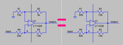
....A negative impedance converter ....the input impedance formula is: - R1 * R3 / R2 ... Here that's - 15k x 10k / 5k = -30k....
Well, yeah, all true.... but an insignificantly different set of values makes a plain ordinary everyday no-negative Differential Amplifier.
Attachments
Setting the reference input to the output of a differential amp is quite a change though.
Note the topology of these circuits has infinite noise gain, whereas a differential amp doesn't.
Note the topology of these circuits has infinite noise gain, whereas a differential amp doesn't.
I'm back working on this topology, combining it with lateral FET output stage, and simplifying the opamp bootstrapping to avoid the transistors, just capacitively bootstrapping direct from the output with some attenuation. The only discrete transistors are the output FETs in fact.
The circuit:

In simulation I get these open and closed-loop responses:


This simulates with distortion of 0.000666% for 1kHz, and 0.002907% at 10kHz (1V peak input into 8 ohm)
The noise analysis yields:

With a simulated square wave (1µs rise/fall), at various amplitudes I get:


Not as well-behaved as I'd like...
The breadboarded prototype is pretty close to this circuit, and seems to work (albeit rather temperamentally) I've not been able to load it at high power but it handles 8 ohm dummy load at lower powers and no-load also. Here's a band-limited square wave test on no-load:

The cyan and purple are the bootstrapped opamp rails, green is input at 500mV/div, yellow is output at 10V/div
The circuit:
In simulation I get these open and closed-loop responses:
This simulates with distortion of 0.000666% for 1kHz, and 0.002907% at 10kHz (1V peak input into 8 ohm)
The noise analysis yields:
With a simulated square wave (1µs rise/fall), at various amplitudes I get:
Not as well-behaved as I'd like...
The breadboarded prototype is pretty close to this circuit, and seems to work (albeit rather temperamentally) I've not been able to load it at high power but it handles 8 ohm dummy load at lower powers and no-load also. Here's a band-limited square wave test on no-load:
The cyan and purple are the bootstrapped opamp rails, green is input at 500mV/div, yellow is output at 10V/div
Attachments
Last edited:
- Home
- Amplifiers
- Solid State
- NIC opamp VAS topology