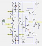
Here is the buffer working att +/- 42 Volt.
Distortion at 1 Watt RMS is THD 0.00007%.
At more power out THD is typically 0.00018%.
The drop out voltage mostly from the MOSFETs is between 6 and 7 Volt from the supply rails.
This is a very good Power Buffer!
Distortion at 1 Watt RMS is THD 0.00007%.
At more power out THD is typically 0.00018%.
The drop out voltage mostly from the MOSFETs is between 6 and 7 Volt from the supply rails.
This is a very good Power Buffer!
Attachments
in one of "thinkhlin" circuits there was som kind of crosscoupling.. Think that with some work could form some kind of error correction... have you explored that..??
If you want to add a deterministic bias control, you can pick some ideas from here:I will post some working circuits. Just want to make them better first. But why dont you try my idea in SPICE. There is room for improvement when there are more than one head in use.
http://www.diyaudio.com/forums/solid-state/218689-cfb-topology-superior-why-22.html#post3222496
Here is the buffer working att +/- 42 Volt.
Distortion at 1 Watt RMS is THD 0.00007%.
At more power out THD is typically 0.00018%.
Thoses numbers are dependent of the generator output Z
wich in your schematics is modelled as being 0R unless
i did miss something.
Since the source can not have nulled output Z the THD
ratios at high frequencies will be much higher.
Lineout,
Can you please how you determine the current through the bias generator compared to the two input transistors? You have 20mA through the input npn/pnp, and another 20mA through the bias gen, but how do you define this current?
Cheers,
Hugh
Can you please how you determine the current through the bias generator compared to the two input transistors? You have 20mA through the input npn/pnp, and another 20mA through the bias gen, but how do you define this current?
Cheers,
Hugh
Last edited:
I repost my circuit.
The previous was not fully stable.
This one is.
With 0.00004% THD
great! I just need a high-performance output stage!
there is similar idea in japan with complementary JFET instead of 4 BJTs.
Voltage-mirror 2SJ113/2SK399 SEPP stereo power amplifier
Voltage-mirror 2SJ113/2SK399 SEPP stereo power amplifier
I had also a great interest with similar output stage based on PMA (Pavel Macura) amplifier, because of the lower THD. I gave up because the DC offset required an output cap.
Jay.
Yes, one of the issues of this output buffer is that it can have some DC offset.
For me there is nothing wrong with solving this by use an output capacitor.
Today's caps are very precise and good. We can use 4700u-10000uF for 8 Ohm.
Many good amplifiers use output cap. And they are still loved by the owners.
Nelson Pass is one great designer using output caps.
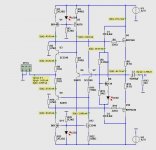
Buffer, see diagram for current version, shows very good THD figures.
The diagram are levels for idle.
Here is my testing in SPICE:
The THD for 4Vp 1 Watt is low.
It is because Buffer works in CLASS A at low levels.
It also tells us that this buffer would do great in pure CLASS A operation!
Yes, one of the issues of this output buffer is that it can have some DC offset.
For me there is nothing wrong with solving this by use an output capacitor.
Today's caps are very precise and good. We can use 4700u-10000uF for 8 Ohm.
Many good amplifiers use output cap. And they are still loved by the owners.
Nelson Pass is one great designer using output caps.
Buffer, see diagram for current version, shows very good THD figures.
The diagram are levels for idle.
Here is my testing in SPICE:
The result for 36Vp shows that we need at least 7 Volt to give room for MOSFET and the transistors.Power Supply +/-42 Volt, 8 Ohm load
04 Vp, 01 Watt THD 0.00008%
08 Vp, 04 Watt THD 0.00032%
12 Vp, 09 Watt THD 0.00036%
16 Vp, 16 Watt THD 0.00031%
20 Vp, 25 Watt THD 0.00029%
24 Vp, 36 Watt THD 0.00027%
28 Vp, 49 Watt THD 0.00026%
32 Vp, 64 Watt THD 0.00029%
34 Vp, 72 Watt THD 0.00039%
35 Vp, 76 Watt THD 0.00045%
36 Vp, 81 Watt THD 0.10755%
The THD for 4Vp 1 Watt is low.
It is because Buffer works in CLASS A at low levels.
It also tells us that this buffer would do great in pure CLASS A operation!
Attachments
It also tells us that this buffer would do great in pure CLASS A operation!
I did it in class-A, because I don't believe in HEXFET in class-B.
I did it in class-A, because I don't believe in HEXFET in class-B.
Believing is religion not technic.
Believing is religion not technic.
I know. I just don't want to build all amplifiers. So I had to make assumptions of what could be a good amp and what not.
I know. I just don't want to build all amplifiers. So I had to make assumptions of what could be a good amp and what not.
That’s fair enough, but keep it for your self otherwise someone can accept is as a fact. Look at Cordell site where HEXFET are used in a class B with great result.
The quality of the messages are dependent upon the quality of the messenger, isn't it? People need to learn the messengers. Then there is no problem. It is as it is.That’s fair enough, but keep it for your self otherwise someone can accept is as a fact..
Look at Cordell site where HEXFET are used in a class B with great result.
Is it any better than your modified JLH? 😀
Lets not twist and fight.
Especially about something off topic.
My latest version in SPICE shows even some better figures. I have increased the current through the input.
1. My question now is who will be the first to build such a buffer?
2. Can somebody find a good name for it? Not necessarily Lineup's Buffer 😀
Especially about something off topic.
My latest version in SPICE shows even some better figures. I have increased the current through the input.
1. My question now is who will be the first to build such a buffer?
2. Can somebody find a good name for it? Not necessarily Lineup's Buffer 😀
Hi Guys
A very cool design! The advantages of class-A operation are huge especially for normal listening levels <1W and so, with no crossover distortion. The Cordell amp referred to has a class-A region of about 180mW with its 150mA idle current.
Did you say what the idle current is for the output devices?
Can we see a plot or just figures for 20kHz THD?
Also, THD vs output <1W?
Any idea of output-z? DF at 8R vs frequency? IM?
A BJT version should offer lower output impedance and THD.
With the complimentary-ness of this circuit, device matching might be critical for best performance - something simulations assume with 'ideal' devices. The current sources need good matching to not skew the DC offset at the output, which of course provides a simple solution for adding such correction: allow a DC servo to adjust one current source to set output DC to zero. The servo can be discrete or opamp.
An alternative DC offset tie-in point is to the input node itself via a resistor from the servo.
Have fun
Kevin O'Connor
londonpower.com
Last edited:
Struth.
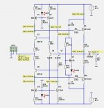
I run my simulation at 275mA bias of the MOSFETs.Can be seen in my diagram.
550mA out into 8 Ohm means peak 4.4 Volt. 4 Volt peak is same as 1 Watt.
With this bias the max distortion is at 12Vp= 9 Watt.
I can give you figures for 20kHz THD.
Less than 1 Watt I can do, too.
Output Z and damping factor I leave to others.
I have told earlier that this circuit is possible with BJT output.
In order to keep input impedance high, we need bipolar drivers + BJT output devices coupled in darlington.
The input impedance of following MOSFET circuit is like 6k.
I call this version 4e.
There is now 40mA in the input and 20mA in the Vbe multiplier.
The THD is as follows:
Power Supply +/-42 Volt, 8 Ohm load 4e
04 Vp, 01 Watt THD 0.00015%
08 Vp, 04 Watt THD 0.00027%
12 Vp, 09 Watt THD 0.00029%
16 Vp, 16 Watt THD 0.00026%
20 Vp, 25 Watt THD 0.00024%
24 Vp, 36 Watt THD 0.00023%
28 Vp, 49 Watt THD 0.00023%
32 Vp, 64 Watt THD 0.00024%
34 Vp, 72 Watt THD 0.00026%
35 Vp, 76 Watt THD 0.00029%
36 Vp, 81 Watt THD 0.04848%
Attachments
Last edited:
Hi Guys
Obviously increasing the front-end currents allows quicker charge and discharge of the mosfet capacitances, improving control over the output 'positioning' and reducing distortion at high signal levels. That is typical with mosfet circuits, where the often thrown-away current buffer into the gates is added back in improving performance.
Doubling the input currents seems to have doubled the THD at 1W even though THD above that level has reduced.
One option that might be worth investigating, is to add a BJT buffer to drive the gates of the mosfet. This would allow operating the front end at lower current while retaining the fast gate drive. I'm not certain if it would be better or worse than the current version of your buffer. Maybe the increase in currents you have now helps to keep device transconductance more constant and reduce gm-variation related distortions?
It's a cool design - actually a hot design!
Have fun
Kevin O'Connor
londonpower.com
Last edited:
- Status
- Not open for further replies.
- Home
- Amplifiers
- Solid State
- New Lineup IDEA - Power Follower/Output stage