Is anyone going to purchase a copy and write a review?
The publisher is New Generation Publishing (see: Self Publishing for UK Independent Authors >> New Generation publishing). Kudos to the author for putting pen to paper! May his entrepreneurship find just financial reward.
Is anyone going to purchase a copy and write a review for the rest of us? If it is a useful text maybe we can get the diyAudio store to stock a few copies.Beware of what you find on internet.
The publisher is New Generation Publishing (see: Self Publishing for UK Independent Authors >> New Generation publishing). Kudos to the author for putting pen to paper! May his entrepreneurship find just financial reward.
I've been among the thirty names on the "To:" line of emails sent out by Michael Kiwanuka, quite a few times. Those experiences lead me to conclude that I will not purchase a copy of this book ... ... unless one becomes available on the used book market, priced less than USD 6.99 including shipping.
Buying used books from previous owners, generates zero additional revenue for author and publisher.
_
Buying used books from previous owners, generates zero additional revenue for author and publisher.
_
Last edited:
Around 2005, Michael Kiwanuka expressed the same perplexity about the term CFA that I had previously expressed in a post here. In 2017 in AudioXpress, he clearly explained why the function attributed to the term for the past forty years was spurious (Peter Baxandall and Ed Cherry had done the same around 1990). I opened a thread here about it shortly afterwards.
I know this, I even posted a few posts in that thread.😉
Stein
As they say, the proof of the pudding is in the eating. Perhaps it might be a good idea to read it before passing judgment.
Yes Michael.
Michael attacked me (I like fighting, so I enjoyed it) in an article in AX about 4 yrs ago, claiming that the CFA diamond buffer ran in class B. It does not. Here is my rebuttal
CFA Diamond Buffer IPS: Does it Operate in Class B or class A?
CFA Diamond Buffer IPS: Does it Operate in Class B or class A?
Fascinating, but one question immediately springs to mind: if the input stage of a CFA runs in Class-A and not Class-AB, where, then, does the current necessary to slew the capacitance at the output of its current mirrors to, say, 2000 V/uS come from? As you are doubtless aware, CFAs routinely achieve such high slew rates.Michael attacked me (I like fighting, so I enjoyed it) in an article in AX about 4 yrs ago, claiming that the CFA diamond buffer ran in class B. It does not. Here is my rebuttal
CFA Diamond Buffer IPS: Does it Operate in Class B or class A?
Note that if this notional CFA has 30pF capacitance to ground at the output of its current mirrors, then 60mA would be required to slew it to 2000V/uS. How would this current be delivered if the input section of the CFA is biased in Class-A, and not Class-AB, at all times?
Clearly, it seems to me, the CFA would either have to be biased at a quiescent current of at least 60mA if it is to remain in Class-A at all times, or its input stage would have to be biased in Class-AB, or even Class-B. It is axiomatic that the quiescent current of all monolithic CFAs is typically of the order of microamperes, yet the slew rate of many of them is in the thousands of volts per microsecond, so the notion that the input section of these devices is biased in Class-A is simply not credible.
Incidentally, your paper on amplifier grounding and layout is really rather good.
https://www.amazon.co.uk/Analytical...ichael+kiwanuka&qid=1639123835&s=books&sr=1-1
ERRATA:
1. The differential pairs of transistors in the transimpedance stages (TIS) of those amplifiers with a folded cascode differential TIS in the book must have reverse-biased (catching) diodes connected across each of their base-emitter junctions to prevent them from being destructively reverse biased when the amplifier is overdriven.
2. To guarantee low-frequency stability, the resistors in the RC filters in the supplementary power supply rails of all the power amplifiers in the book, particularly those in the positive rails, should not exceed 10 Ohms.
Please find attached the LTspice files of the revised amplifiers.
Attachments
The current required to slew the TIS comp cap comes from the feedback resistor which also forms part of the amps compensation network. On IC’s, the gm of the DB output pair is very high. On a power amp for practical reasons it’s usually about 200-300 V/us. If you want higher slew rates you would need to keep the degen resistors low in value (a few ohms at most) and match the 4 DB transistors like you do on IC’s so you don’t get offset problems. I design for 1-2 V/us per peak output voltage so 100-300 V/us is fine for a big amp.Fascinating, but one question immediately springs to mind: if the input stage of a CFA runs in Class-A and not Class-AB, where, then, does the current necessary to slew the capacitance at the output of its current mirrors to, say, 2000 V/uS come from? As you are doubtless aware, CFAs routinely achieve such high slew rates.
Note that if this notional CFA has 30pF capacitance to ground at the output of its current mirrors, then 60mA would be required to slew it to 2000V/uS. How would this current be delivered if the input section of the CFA is biased in Class-A, and not Class-AB, at all times?
Clearly, it seems to me, the CFA would either have to be biased at a quiescent current of at least 60mA if it is to remain in Class-A at all times, or its input stage would have to be biased in Class-AB, or even Class-B. It is axiomatic that the quiescent current of all monolithic CFAs is typically of the order of microamperes, yet the slew rate of many of them is in the thousands of volts per microsecond, so the notion that the input section of these devices is biased in Class-A is simply not credible.
Incidentally, your paper on amplifier grounding and layout is really rather good.
Anyway, in my rebuttal I show plots and also why the DB is a practical power amp never leaves class A.
Please also see AoE for a general discussion on CFA’s and the references on my site to some papers describing operation in much greater detail than I can do justice to the subject.
Peace and thanks for your comments on the GL presentation.
Yes, the current required to slew the compensation capacitor must of necessity be sunk by and sourced from the feedback resistor by the input section of the CFA, but in order to sink and source the tens of milliamps required to slew the compensation capacitor, the input section of the CFA must necessarily slide from Class-A, if it was so biased, to Class-B.The current required to slew the TIS comp cap comes from the feedback resistor which also forms part of the amps compensation network. On IC’s, the gm of the DB output pair is very high. On a power amp for practical reasons it’s usually about 200-300 V/us. If you want higher slew rates you would need to keep the degen resistors low in value (a few ohms at most) and match the 4 DB transistors like you do on IC’s so you don’t get offset problems. I design for 1-2 V/us per peak output voltage so 100-300 V/us is fine for a big amp.
Anyway, in my rebuttal I show plots and also why the DB is a practical power amp never leaves class A.
Please also see AoE for a general discussion on CFA’s and the references on my site to some papers describing operation in much greater detail than I can do justice to the subject.
Peace and thanks for your comments on the GL presentation.
No, that is not correct for a power amplifier. In my rebuttal, I point out that in IC amplifiers this may bell be the case - the IC DB gm is very high, little or no emitter degeneration is used in the DB output pair with designers instead relying on the closely matched device parameters you can only get in an IC fabrication process to achieve the good DC balance and tracking you need if you are to dispense with the degeneration resistors. In this type of device, the DB may well transition to class B (I don't know, I have not analyzed it or sim'd it) and is somewhat analogous to an undegenerated VFA long tail pair where very fast high input signal transients cause one of the input devices to switch off while the other conducts the full tail current.
In all my CFA power amps, the gm is lower because the degen resistors are 150 Ohms - this to ensure the DB is well balanced at DC with device currents all set to 1mA because the voltage drops across the 150 Ohm resistors swamp Vbe differences by a large margin. It is still possible to build power amps with this approach with 250V/us SR's (see here https://www.ovationhifidelity.com/product/model-1721/). The DB output current can go >8x the standing current and still remain in class AB for all signal levels over a bandwidth up to 250kHz. (Note I use the term SR but it is more accurately described as rise/fall time since CFA's do not SR limit in the same way VFA's do).
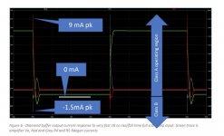
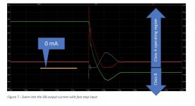
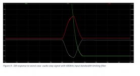
You can see in the plots below that with a 400 kHz BW limited amplifier and 2us rise/fall time stimulus (already much wider BW and faster rise/fall times than you will ever encounter in practice) the amplifier remains in class A. You only go into class AB with ultrafast rise/fall times and not input BW limiting filter.
In all my CFA power amps, the gm is lower because the degen resistors are 150 Ohms - this to ensure the DB is well balanced at DC with device currents all set to 1mA because the voltage drops across the 150 Ohm resistors swamp Vbe differences by a large margin. It is still possible to build power amps with this approach with 250V/us SR's (see here https://www.ovationhifidelity.com/product/model-1721/). The DB output current can go >8x the standing current and still remain in class AB for all signal levels over a bandwidth up to 250kHz. (Note I use the term SR but it is more accurately described as rise/fall time since CFA's do not SR limit in the same way VFA's do).
You can see in the plots below that with a 400 kHz BW limited amplifier and 2us rise/fall time stimulus (already much wider BW and faster rise/fall times than you will ever encounter in practice) the amplifier remains in class A. You only go into class AB with ultrafast rise/fall times and not input BW limiting filter.
Attachments
Last edited:
What, precisely, is the point of CFAs in audio frequency applications?No, that is not correct for a power amplifier. In my rebuttal, I point out that in IC amplifiers this may bell be the case - the IC DB gm is very high, little or no emitter degeneration is used in the DB output pair with designers instead relying on the closely matched device parameters you can only get in an IC fabrication process to achieve the good DC balance and tracking you need if you are to dispense with the degeneration resistors. In this type of device, the DB may well transition to class B (I don't know, I have not analyzed it or sim'd it) and is somewhat analogous to an undegenerated VFA long tail pair where very fast high input signal transients cause one of the input devices to switch off while the other conducts the full tail current.
In all my CFA power amps, the gm is lower because the degen resistors are 150 Ohms - this to ensure the DB is well balanced at DC with device currents all set to 1mA because the voltage drops across the 150 Ohm resistors swamp Vbe differences by a large margin. It is still possible to build power amps with this approach with 250V/us SR's (see here https://www.ovationhifidelity.com/product/model-1721/). The DB output current can go >8x the standing current and still remain in class AB for all signal levels over a bandwidth up to 250kHz. (Note I use the term SR but it is more accurately described as rise/fall time since CFA's do not SR limit in the same way VFA's do).
You can see in the plots below that with a 400 kHz BW limited amplifier and 2us rise/fall time stimulus (already much wider BW and faster rise/fall times than you will ever encounter in practice) the amplifier remains in class A. You only go into class AB with ultrafast rise/fall times and not input BW limiting filter.
Lets not go down that rabbit hole!
Its simply an amplifier topology that happens to possess certain characteristics just like a VFA has certain characteristics. I am comfortable designing with CFA's and have stuck with that since 2012. Nothing more, nothing less.
Its simply an amplifier topology that happens to possess certain characteristics just like a VFA has certain characteristics. I am comfortable designing with CFA's and have stuck with that since 2012. Nothing more, nothing less.
Of course I respect your right to use any topology of your choice. However, I am of the view that the choices made by those designers seeking the very best performance should be informed by the characteristics and, therefore, suitability of each topology under consideration for the purpose of audio frequency amplification.Lets not go down that rabbit hole!
Its simply an amplifier topology that happens to possess certain characteristics just like a VFA has certain characteristics. I am comfortable designing with CFA's and have stuck with that since 2012. Nothing more, nothing less.
The most important failing of the standard CFA insofar as audio frequency amplification is concerned is its paucity of forward-path gain. This is due to the fact that all of its forward-path gain is generated only by a single common-emitter stage. This means that not enough loop gain is generated to ameliorate the amplifier’s forward-path non-linearity, especially that of the output stage, when the major feedback loop is closed. This also explains, at least in part, this topology's poor PSRR and mediocre DC offset. Moreover, the standard CFA does not benefit from the linearisation afforded by Miller minor negative feedback loop frequency compensation in its various forms that is applicable to the classic two-stage topology with a differential pair as its input stage.
Therefore, I contend that the CFA would not be considered by anyone for use in audio frequency applications if sound engineering principles were the only criteria influencing the decision. In fact, as far as audio frequency amplification is concerned, the simple differential pair, with a current mirror as its load, driving a transimpedance stage remains the optimum solution for generating adequate forward-path gain with good linearity.
I see lots of folks chasing single digit ppm distortion. It’s a waste of time and energy. Despite claims to the contrary, no one can hear anything below about 0.01% and I am being very generous here - 0.1 to 0.5 is more like it (I only consider fully documented and scientifically conducted DBT - people claiming this or that without a proper test set-up are a complete nonsense )
Anyway, there are plenty of high loop gain CFA designs on the forum - see dadod for example- if that floats your boat.
How much loop gain do you need? A good modern amp will be about 0.5% open loop, place 70 or 80 dB loop gain around that using TMC or similar and you are at 10-30 ppm distortion at close to full power at HF. If you need much more loop gain than this to get to the figures I mention, then you have other issues. Surely getting low distortion with minimal feedback should be the goal we chase, not huge amounts to try to correct a flawed design?
Last edited:
Yes, nobody is likely to hear even 1% THD at 20 KHz, but that shouldn't stop progress in the field. Indeed, it could be argued that a Model-T Ford is perfectly adequate for most people, but that has not stopped technological advancements being made in the automotive industry over the past century.I see lots of folks chasing single digit ppm distortion. It’s a waste of time and energy. Despite claims to the contrary, no one can hear anything below about 0.01% and I am being very generous here - 0.1 to 0.5 is more like it (I only consider fully documented and scientifically conducted DBT - people claiming this or that without a proper test set-up are a complete nonsense )
Anyway, there are plenty of high loop gain CFA designs on the forum - see dadod for example- if that floats your boat.
How much loop gain do you need? A good modern amp will be about 0.5% open loop, place 70 or 80 dB loop gain around that using TMC or similar and you are at 10-30 ppm distortion at close to full power at HF.
In my opinion, the goal should be to generate as much forward-path gain as possible with as much forward-path linearity as possible from as few forward-path gain stages as possible (to minimise forward-path poles) and then apply as much major loop negative feedback as possible without compromising acceptable major feedback loop stability margins. The late Professor James Roberge demonstrated decisively that two stages of forward-path gain are the optimal compromise.Surely getting low distortion with minimal feedback should be the goal we chase, not huge amounts to try to correct a flawed design?
Last edited:
Yes, nobody is likely to hear even 1% THD at 20 KHz, but that shouldn't stop progress in the field. Indeed, it could be argued that a Model-T Ford is perfectly adequate for most people, but that has not stopped technological advancements being made in the automotive industry over the past century.
As in most things, there is much latitude for interpretation and personal judgement. We should leave it at that and seek perfection in our chosen paths.
🙂
🙂
I see lots of folks chasing single digit ppm distortion. It’s a waste of time and energy. Despite claims to the contrary, no one can hear anything below about 0.01% and I am being very generous here - 0.1 to 0.5 is more like it (I only consider fully documented and scientifically conducted DBT - people claiming this or that without a proper test set-up are a complete nonsense )
Anyway, there are plenty of high loop gain CFA designs on the forum - see dadod for example- if that floats your boat.
This is one of CFA with high LG, is this enough high?

- Status
- Not open for further replies.
- Home
- Amplifiers
- Solid State
- New book on amplifier design.