Hi everyone,
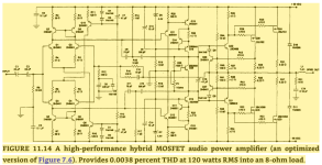
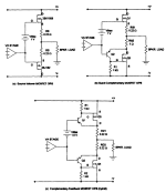
I may have started my project with to much self confidence. I read the entire book "High-Power Audio Amplifier Construction Manual" from G. Randy Slone. I choose to build the High-performance Hybrid MOSFET Audio Power Amplifier from Figure 11.14. (See first image).
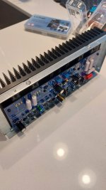
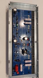
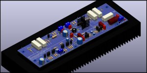
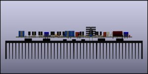
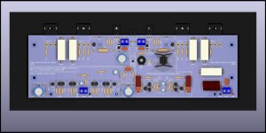
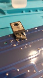
I redraw the entire drawing into the KiCad software (Linux) and created the PCB in the same suite software and have had it manufactured by PCBWay in China. It is my first experience as designing an audio PCB but I have a lot of experience with creating PCBs. I'll attach a picture of my drawing and a PCB capture, as well as some 3D views from KiCad PCB and some pictures of my final PCB. I share those for you to have as much as information to help me.
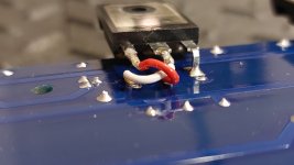
Now, my first mistake was with the orientation of the two upper MOSFETs. The original figure 11.14 doesn't specify the Drain and Source pin. The only note is the line going to the Gate. The upper MOSFETs have their lines over the center of the part while the lower ones have their lines under the center of the part. Unfortunately, in my software the library have the Source line in the center of the part. So I didn't notice this and even if I rechecked everything two and three times; shame on me, I didn't realized that mistake. It is my first experience with MOSFET, gee... I guess we learn from ours mistakes. Anyway, I was able to use my PCBs by crossing both Source and Drain pins of the upper MOSFETs.
After having fix this, I got the right +VCC and -VCC voltages. I use two Rigol DP712 Power Supply so I can start applying voltages from +/- 5 VDC and going up. But I cannot go more than +/- 8 VDC before the positive section of the Sine wave start to reach a limit as if the +rail limit was reached. Here I don't understand why this is happening when I actually do raise the Power Supply! And the more I raise it, the more the sin wave distord until the output signal goes off. I bet the MOSFET turn off from their internal protection.
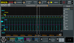
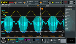
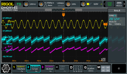
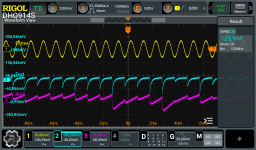
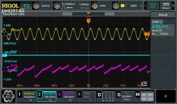
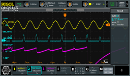
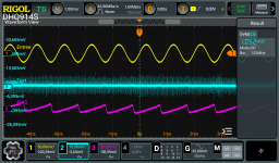
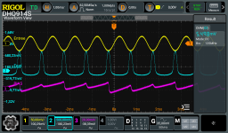
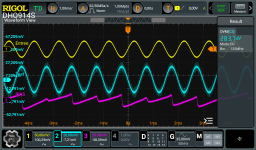
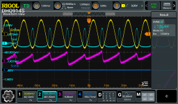
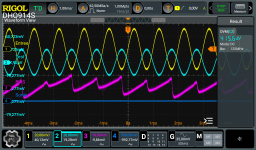
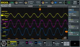
I captured some screenshots from my Rigol DHO914S scope. It is a four traces scope. The trace 1 (yellow) is the input signal from my Rigol Generator, a 60 mV,1 kHz sin wave. The trace 4 (Blue) is the output of the Amplifier. The trace 3 (Rose) is the BIAS and finally I used the trace 2 (Cyan) as the testing probe in the circuit. This latest is what concerned me. I trace the signal starting from the Input and as I soon as I reach collector of Q101, I get this really weird signal, an envelop synced with the output signal. So I start to ask myself if this could be due to a very bad PCB design or if it is a result of a faulty part. This is where I ask your help. Maybe some of you are already familiar with this kind of weird signal. I took a zoom of the weird envelop and used the Cursors to measure the frequency and the level. That is the latest capture image; I read -401.5mV as delta Y and a frequency of 4.409MHz !
Any idea what could cause this? Could it be generated by my Drain and Source crossing?
My very best regards,
Yves
I may have started my project with to much self confidence. I read the entire book "High-Power Audio Amplifier Construction Manual" from G. Randy Slone. I choose to build the High-performance Hybrid MOSFET Audio Power Amplifier from Figure 11.14. (See first image).
I redraw the entire drawing into the KiCad software (Linux) and created the PCB in the same suite software and have had it manufactured by PCBWay in China. It is my first experience as designing an audio PCB but I have a lot of experience with creating PCBs. I'll attach a picture of my drawing and a PCB capture, as well as some 3D views from KiCad PCB and some pictures of my final PCB. I share those for you to have as much as information to help me.
Now, my first mistake was with the orientation of the two upper MOSFETs. The original figure 11.14 doesn't specify the Drain and Source pin. The only note is the line going to the Gate. The upper MOSFETs have their lines over the center of the part while the lower ones have their lines under the center of the part. Unfortunately, in my software the library have the Source line in the center of the part. So I didn't notice this and even if I rechecked everything two and three times; shame on me, I didn't realized that mistake. It is my first experience with MOSFET, gee... I guess we learn from ours mistakes. Anyway, I was able to use my PCBs by crossing both Source and Drain pins of the upper MOSFETs.
After having fix this, I got the right +VCC and -VCC voltages. I use two Rigol DP712 Power Supply so I can start applying voltages from +/- 5 VDC and going up. But I cannot go more than +/- 8 VDC before the positive section of the Sine wave start to reach a limit as if the +rail limit was reached. Here I don't understand why this is happening when I actually do raise the Power Supply! And the more I raise it, the more the sin wave distord until the output signal goes off. I bet the MOSFET turn off from their internal protection.
I captured some screenshots from my Rigol DHO914S scope. It is a four traces scope. The trace 1 (yellow) is the input signal from my Rigol Generator, a 60 mV,1 kHz sin wave. The trace 4 (Blue) is the output of the Amplifier. The trace 3 (Rose) is the BIAS and finally I used the trace 2 (Cyan) as the testing probe in the circuit. This latest is what concerned me. I trace the signal starting from the Input and as I soon as I reach collector of Q101, I get this really weird signal, an envelop synced with the output signal. So I start to ask myself if this could be due to a very bad PCB design or if it is a result of a faulty part. This is where I ask your help. Maybe some of you are already familiar with this kind of weird signal. I took a zoom of the weird envelop and used the Cursors to measure the frequency and the level. That is the latest capture image; I read -401.5mV as delta Y and a frequency of 4.409MHz !
Any idea what could cause this? Could it be generated by my Drain and Source crossing?
My very best regards,
Yves
Attachments
-
 Capture d’écran du 2023-09-21 08-44-06.png58.8 KB · Views: 1,043
 -
 RigolDS0.png50.2 KB · Views: 769
 -
 RigolDS1.png57.5 KB · Views: 453
 -
 20231017_140047.jpg299.4 KB · Views: 454
 -
 20231017_140037.jpg385 KB · Views: 425
 -
 06-Figure 11.14.Rev1.0.jpg189.4 KB · Views: 402
 -
 02-Figure 11.14.Rev1.0.jpg138.4 KB · Views: 401
 -
 01-Figure 11.14.Rev1.0.jpg182.8 KB · Views: 480
 -
 Figure 11.14 Rev1.0.png111.5 KB · Views: 846
Unfortunately you have CFP output stage which is the hardest type to stabilize. One thing to check is that you have correct bias current flowing in the outputs - too little and instability of the main loop is likely - too much and things get hot really fast. Dial down the current limit on your supplies to the minimum you need as you go to prevent damage as you experiment. You might want to try some base resistance on the driver transistors.
Can you experiment with the output stage in isolation?
I'd also check that you've not blown those MOSFETs as the waveforms look rather asymmetric.
I'd always breadboard a design first rather than go to PCB without physically testing.
Can you experiment with the output stage in isolation?
I'd also check that you've not blown those MOSFETs as the waveforms look rather asymmetric.
I'd always breadboard a design first rather than go to PCB without physically testing.
This amp design has a number of "problems".
1. It is a symmetric IPS, which causes unpredictable VAS current. This amp has current limits on the VAS, but that does not make the operating VAS current predictable.
2. The output is "CFP". This can work but it also can be a stability headache and is load dependent.
3. It uses VI output protection. VI protection is typically unstable and very load dependent.
4. The IPS CCS's need supply noise filtering.
In short, it is a very poor choice for a beginner. It is a collection of "cool" ideas that lack a greater wisdom. I suspect an expert could make it work but even then, it would not be particularly reliable, ie you would be constantly rebuilding it. Which is, after all, what audiophiles do.
What do you mean exactly? Removed them from the PCB?Can you experiment with the output stage in isolation?
I have bought 8 MOSFETs from the beginning in the goal to build a stereo system. I have 2 NPN MOSFETs and 2 PNP MOSFETs by board. When I found the problem with the Drain and Source of the upper MOSFET inverted, I installed them by crossing their pins with wires. But I was not confident with the result. And I already had the weird phenomenon, well is wasn't that ugly. So I thought that I could have burn the MOSFETs. Then I decided to use the others one bought for the other channel, and I installed two new MOSFET on the board. Only one PNP and one NPN. This time, because the pin wasn't cuted yet, I was able to used plier to cross the pin to invert Source and Drain, So since they are new, I am pretty sure their are good and didn't suffer from my preceding tests.I'd also check that you've not blown those MOSFETs as the waveforms look rather asymmetric.
I will try though to limit the current much to a lower value to see the effect.
As for the BIAS, I have a 620 Ohms in series with the 1 kOhms trim-pot. I have to lower the trim-pot to the minimum to keep the Sin waveform clean. I even tried to solder a second 620 Ohms in parallel to the first one but without apparent difference. So you suggest to add a resistor in series with the base of the driver? Those are Q502 and Q602, right?
🙄 Now you confirm my first impression... I quote myself...In short, it is a very poor choice for a beginner.
I may have started my project with to much self confidence.
Regardless of the problems, it looks like you did a great job building this amplifier module. I can't tell from your scope traces if there's a DC offset problem? Did you measure the DC output voltage with no signal? I would concentrate on the clipping issue before looking into the oscillation issue.
H
HAYK
not a good design for a begineer; it has inherent design problems as mentioned by stevu that should have been dealt with first.
H
HAYK
The Amp is already built with much effort, it is not the time for lamentation but resolution. The fellow is asking help to make it function not opinion about his choice.

Thank you kramtweeter! I must say that I am proud of it.Regardless of the problems, it looks like you did a great job building this amplifier module.
I made progress, but first I think it is time for me to share all the procedure steps and mistakes I made chronologically... So from the beginning:
- I did a spot check of the Rails of the PCB without any parts mounted.
- I soldered all the pieces and did a first test applying the DC voltages starting from +/- 5 VDC on the rails. There my negative Power Supply was showing 0,00 VDC. So something was wrong. It is then that I studied back all the schematics and found the Drain-Source orientation of the PNP MOSFET from Figure 6.6 (c) of the book (Picture below).
- I fixed the orientation soldering two wires on the pins of the 2 PNP MOSFETs and did a test. (Picture of the wires below). There the rails voltages was corrects. I was able to raise them to +/-20 VDC with two 8 Ohms resistors 50 Watts on the output. Then I raised the frequencies and at frequencies above 5 kHz ( if I remember well ) some oscillations was starting, so I stopped there.
- Suspecting that maybe my wires fix could be the oscillation problem, I choose to remove all the four MOSFETs and started with two new MOSFETs, one NPN and one PNP, this latest by bending it's Drain and Source pins with pliers instead of using wires. ( Picture below ). But before proceeding with this new setup, I thought to do new tests without the MOSFETs, thinking to preserve them. Big mistake! The two 47 Ohms 5 watts started to make fume! I stop it right there and measure them. They were still in the specifications range ; 46,5 Ohms for one and 45,9 Ohms for the other one.
- So I soldered the two new MOSFETs above. With this new setup, I got the weird sine wave from my starting description of this blog.
- Then I replaced the three 2N5551 transistors Q401, Q402, Q403, as they were the one from I could see the bad signal on the scope. Nothing changed.
So yesterday night, after having read Mark Tillotson comments above, I noticed that I had the sine wave present on the rails voltages! I started to have real doubts about the 47 Ohms resistors and all the transistors around them. This morning I replaced the two 47 Ohms resistors R503, R603, the transistors Q1, Q304, Q404, Q502, Q602.
A new test now give absolutely no signal at the output! A straight line with no DC. But the two rails voltages are clean without any weird signal and the BIAS is a straight line to.
I am now suspecting the MOSFETs. Should I proceed and replace them with two new ones? I still have one PNP and one NPN new. But these babies cost a lot! I am a bit scare to try and risk them.
Any advise from there...?
Attachments
Well that is the spirit! Thank you very much ;-)The Amp is already built with much effort, it is not the time for lamentation but resolution. The fellow is asking help to make it function not opinion about his choice.
I just saw your suggestion... So I did it with the actual NPN MOSFET but I used one of the wired MOSFET for the PNP. I didn't want to band again the pin of the PNP MOSFET, it would not be safe to play with them. I did test all MOSFET first and compared their diode test to the two unused new one. I know that for Power MOSFETs the diode test isn't sufficient but I wanted to compare them anyway in case I could find one bad. And I found nothing different from all the used one compared to the new unused ones.Desolder the drains of all outputs. The amp must function without load with full supply.
So I still don't have any output. I probed the signal and here are the capture of the scope below. Be aware that from the upper side and the lower side of the schematics, the channel 2 (my test probe) have different vertical scale.
In order, the images show:
RigolDS0.png Q101 collector
RigolDS1.png Q201 collector
RigolDS2.png Q301 base
RigolDS3.png Q401 base
RigolDS4.png Q301 emitter
RigolDS5.png Q401 emitter
RigolDS6.png Q1 collector
RigolDS7.png Q1 emitter
RigolDS8.png Q301 emitter
RigolDS9.png Q401 emitter
I hope I didn't mistake them ;-)
Attachments
-
 RigolDS9.png69.2 KB · Views: 81
 -
 RigolDS8.png55.4 KB · Views: 91
 -
 RigolDS7.png47.8 KB · Views: 80
 -
 RigolDS6.png47.7 KB · Views: 90
 -
 RigolDS5.png48.1 KB · Views: 79
 -
 RigolDS4.png67.5 KB · Views: 74
 -
 RigolDS3.png52.5 KB · Views: 85
 -
 RigolDS2.png65.8 KB · Views: 94
 -
 RigolDS1.png65.5 KB · Views: 119
 -
 RigolDS0.png67.4 KB · Views: 81
H
HAYK
The outputs MOSFETS are only to amplify the current, the drivers alone should make the amp function without load. You can safely power it up and diagnose the problem without the MOSFETS.
The first thing is DC function with no input, check the driver's temperature and the bias current on R37-38. Measure the VAS current on R23-R24. It should be 5-10ma. Then see the output offset and on scope if there is no oscillations.
PS You can disable the outputs by shorting gate-source.
The first thing is DC function with no input, check the driver's temperature and the bias current on R37-38. Measure the VAS current on R23-R24. It should be 5-10ma. Then see the output offset and on scope if there is no oscillations.
PS You can disable the outputs by shorting gate-source.
Last edited by a moderator:
When I did that at step 4 above, the R503 and R603 started to fume... Maybe something else was wrong then...The outputs MOSFETS are only to amplify the current, the drivers alone should make the amp function without load. You can safely power it up and diagnose the problem without the MOSFETS.
You seem to refer R37-38 from the original schematic. Unfortunately, the quality is so poor that I have a hard time reading most of their references. Could you refer me by using my schematic version. I do understand that you are talking about R504-R604 and drivers Q502-Q602, right? These are on the heat-sink and never came to a sensible temperature on my fingers.The first thing is DC function with no input, check the driver's temperature and the bias current on R37-38.
Again, you mean R304-R404 on my schematic?Measure the VAS current on R23-R24. It should be 5-10ma. Then see the output offset and on scope if there is no oscillations.
Ah doh... lol Good to know lolPS You can disable the outputs by shorting gate-source.
I have no voltage difference across R304 neither across R404. I have 2.1mA across R302 and R402...
I only have 4,1 VDC across both zener. My calculations would require 4,4 VDC as per my schematic. Could it be that that cause the non conduction of VAS?
A partly success!
I guess I was to scared to raise the DC voltages. Following your last suggestion Hayk, I raised the rails voltage to +/- 40 VDC checking the heat of every parts. Nothing came enough hot to sense it with the fingers.
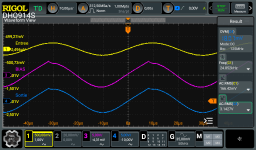
Then I injected the 1kHz signal and hourra! I got a very clean output and BIAS sine wave with no DC voltage at the output (first picture).
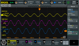
Then I raised the frequency to 5 kHz, and 20 kHz, still clean. At 25 kHz, I could see a start of distortion. Pictures 2 and 3.
I then go down to 5 Hz, still a clean wave.
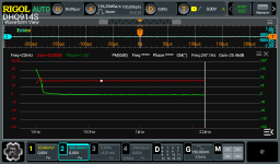
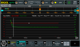
So I decided to test the whole think with my Rigol Bode plot function. For security, I limited the frequency response from 10 Hz to 22 kHz, at 150 mV.
See pictures 4 and 5. Notice how good are the Phase and the Gain with their straight lines. 25.43dB at 20 Hz with 10,06 degrees of phase shift. And 25.58dB at 22kH with -1,36 degrees of phase shift.
P.S. : Not bad for a beginner ;-)
I guess I was to scared to raise the DC voltages. Following your last suggestion Hayk, I raised the rails voltage to +/- 40 VDC checking the heat of every parts. Nothing came enough hot to sense it with the fingers.
Then I injected the 1kHz signal and hourra! I got a very clean output and BIAS sine wave with no DC voltage at the output (first picture).
Then I raised the frequency to 5 kHz, and 20 kHz, still clean. At 25 kHz, I could see a start of distortion. Pictures 2 and 3.
I then go down to 5 Hz, still a clean wave.
So I decided to test the whole think with my Rigol Bode plot function. For security, I limited the frequency response from 10 Hz to 22 kHz, at 150 mV.
See pictures 4 and 5. Notice how good are the Phase and the Gain with their straight lines. 25.43dB at 20 Hz with 10,06 degrees of phase shift. And 25.58dB at 22kH with -1,36 degrees of phase shift.
P.S. : Not bad for a beginner ;-)
Attachments
This is a poor design because it has no control over the bias current in the VAS. The gain is so high that any offset between the two differentials will cause the VAS to either not have any current or too much current.
Look at Leach's amp for a working design. The key is to lower the gain to tolerate mismatch between the complementary halves.
Ed
Look at Leach's amp for a working design. The key is to lower the gain to tolerate mismatch between the complementary halves.
Ed
I am new to this site. Do you have any link?Look at Leach's amp for a working design.
As for the choice of design made, having read the entire book before choosing, I choose this circuit based on the author comments, that I quote below by a capture of the page book...
As a beginner, I simply trusted the author...
Attachments
@Sevy I really hope you will not be getting discouraged from this great hobby and maybe even get this amp to function. Looking at the (1-star) Amazon reviews, I would not be too confident. They say what the knowledgable folks above say, uncontrolled bias etc. Many circuits in the book seem to be really bad.
I cannot read the MOSFET types in the schematic above. A MOSFET amp having exhaustively been discussed here in the forums pretty well suited for beginners is this: https://www.diyaudio.com/community/threads/power-amp-under-development.43331/
Maybe you can recycle enough components to not make this a too bad experience.
- Home
- Amplifiers
- Solid State
- Need helps! Weird signal results on my DIY High-performance Hyrid MOSFET Audio Power Amplifier