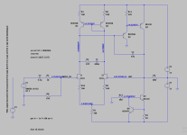
The last simulation has ~67mA or about 1 Watt dissipation on Q4. This is unnecessary and will kill a smaller transistor. Even a BD140 will require a heat sink. You only need a bit more than 15V/600 ~=25mA. And, the negative swing will be limited to Q5 Vb, ie -6.36V, so the max negative output current will be -6/600 = -10mA until Q5 saturates, after which you may get a bit more from R2 but the CCS is no longer working. A better CCS uses a VBE instead of a Zener so that you waste as little collector swing as possible. I would set the current at 30mA so that the heat is reduced, or resort to an AB output.
In any case, there are a lot of great OP-amps available. Granted, it is not easy to cleanly extend them for 600 Ohm or high voltage but for +-15V, they are hard/impossible to beat.
In any case, there are a lot of great OP-amps available. Granted, it is not easy to cleanly extend them for 600 Ohm or high voltage but for +-15V, they are hard/impossible to beat.
Attachments

Any specific reason for using BC847 instead of BC846?A better CCS uses a VBE instead of a Zener so that you waste as little collector swing as possible.
Picking between two JFETS, J310 and J112, which one is better for audio?
According to simulation, I get 0.00136% THD or 0.012% THD+N with J112.
0.047% THD or 0.053% THD+N with J310.
Looks like J112 is better.
According to simulation, I get 0.00136% THD or 0.012% THD+N with J112.
0.047% THD or 0.053% THD+N with J310.
Looks like J112 is better.
Last edited:
How to calculate this?so depending on current of DC around .75 to 1.2 watts
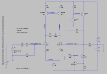
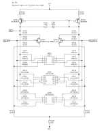
I think I will build two variants: one with J112 and another with 2N7002. Attached is the final schematics that I think I like the most.
Parts count is pretty low. Two JFETS, pair or power BJTs, and four BJTs for current mirror, current source.
Parts count is pretty low. Two JFETS, pair or power BJTs, and four BJTs for current mirror, current source.
Attachments
Last edited:
Not necessarily: Broskie has a number of good options like this one:I guess the ability to drive low loads at low distortions requires a lot of parts…
https://www.tubecad.com/2021/08/blog0543.htm
As shown, it is very hefty and is designed to drive 32 ohm, but you can use ~15x larger resistor values and transistors like BC327/337 or 2N2219/2905
The Taylor follower is also an interesting possibility:
https://www.tubecad.com/2004/blog0023.htm
The subject has been discussed on the forum, here for example:
https://www.diyaudio.com/community/...uffer-as-power-output-stage.2754/post-2043894
Thanks for those links. Something more to read on for me. I started my journey into finding voltage follower buffer by reading this really great article - https://sound-au.com/articles/followers.html

I found LS844 dual JFET in SOIC package on digikey for $9/pc. TI has one for $4. No dual matched J112 though…
I want to make evaluation PCB layout for all of them. Will be fun to measure and to listen to those.
Now I’m thinking of how to make an invering buffer to be able to make balanced signal driver from bd140/bd139 variant…
Now I’m thinking of how to make an invering buffer to be able to make balanced signal driver from bd140/bd139 variant…
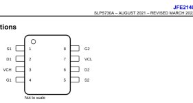
Looking at the JFE2140 and LS844 in soic package.
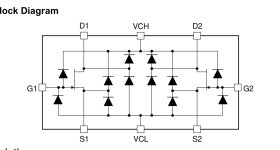
JFE2140 has JFETs G,D,S pins and additionally ESD protection diodes tied to G,D,S, to pin 3 called VCH and to pin 7 called VCL.
For dual 15V supply, do I connect those VCH and VCL pins to GND?
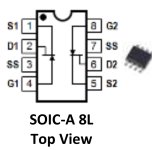
LS844 has the same pinout for G,D,S for JFETs. Pin 3 and pin 7 marked as SS and there is no information on those in the datasheet.
Is it safe to connect SS pins to GND?
JFE2140 has JFETs G,D,S pins and additionally ESD protection diodes tied to G,D,S, to pin 3 called VCH and to pin 7 called VCL.
For dual 15V supply, do I connect those VCH and VCL pins to GND?
LS844 has the same pinout for G,D,S for JFETs. Pin 3 and pin 7 marked as SS and there is no information on those in the datasheet.
Is it safe to connect SS pins to GND?
Attachments
Last edited:
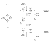
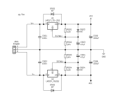
Attached is schematics for the evaluation board. It is balanced XLR input.
Using jumpers one can configure 4 options for input devices:
Any test points to add?
Using jumpers one can configure 4 options for input devices:
- MMBFJ112 (SOT23-3)
- LS844 (dual matched SOT23-6)
- JFE2140 (dual matched SOIC-8)
- 2N7002HSX (dual SOT363)
Any test points to add?
Attachments

An issue I noticed later is that the LTP is not rail-rail so if you want the input to handle +-15, you need to attenuate it and the feedback so that the LTP does not clip.
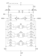
And a Push-pull class-A output can drive 600 Ohms without much heat, but it does not give better THD.
And a Push-pull class-A output can drive 600 Ohms without much heat, but it does not give better THD.
Attachments
My main concern is reasonable low THD in a working range of balanced signal outputs of most audio equipment. For example topping dacs, preamps, my ddj 1000 controller, mixing consoles…
- Home
- Source & Line
- Analog Line Level
- Need help simulating discrete impedance matching buffer in LTSpice - using 2N7002 and BC856