In a simulation your output offset ought to be almost zero. Can you post your schematic?In simulation, changing the 620R to 560R reduces the offset from 77mV to 50mV, and nothing else seems to change, apart from a (very) small reduction in simulated THD.
In a simulation your output offset ought to be almost zero. Can you post your schematic?
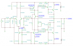
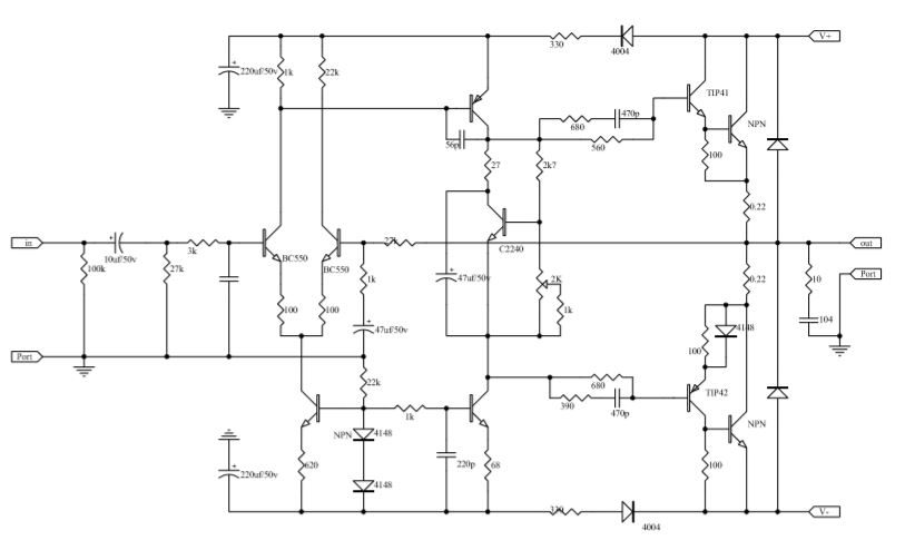
Here it is. My sim package (Tina Pro) doesn't have models form some of the transistors, so I have made some substitutions, which of course is less than ideal. (The actual transistor types are in blue. The TIP3055's are of course 2SC5200!)
I can upload the .sch file if it's any use?
.
Attachments

Last edited:
Referring to the schematic posted below.
I changed:
R1 (27k) to 24k (input shunt resistor)
R22 (3k) to 2.7k (input series resistor)
Q8 - fitted higher HFE than Q7 (LTP)
Offset voltage dropped from around 100mV to 55mV and 65mV.
So still can't get within spec (NCC200 states "less than 50mV").
I also tried reducing R4 (620R) to 560R but that barely even changed the DC offset voltage, so I put it back to 620R.
Attachments
Is VG1 zero ac?
Is the thing stable? Any ac on the output?
It's odd that AM3 and AM4 are so different.
Is the thing stable? Any ac on the output?
It's odd that AM3 and AM4 are so different.
Oh I see the reason AM3 and AM4 are different is because you have an 8 ohm resistor from output to ground. That's ok.
So still can't get within spec (NCC200 states "less than 50mV").
If you look at the circuit, nothing can significantly reduce the offset, except if you modify the VAS. If you look at the VAS transistors (Q4 and Q3), top transistor doesn't have emitter resistor while bottom transistor has 68R emitter resistor. This imbalance tends to move offset to the top or positive side. If you lower the R9=68R, offset will move down but this also means current will be higher. IIRC, original VAS current is 10mA with the ZTX? (Yours is 8.7mA).
You can also balance the top and bottom VAS by adding small resistor on the emitter of top transistor. This might have quality compromises that have to be checked. If there is no space for new R on the pcb, you can attach 1/8W resistor on the transistor's leg.
You can also reduce the negative voltage rail by adding RC network on the negative supply. This will lower currents in LTP and VAS, which means you will need to adjust.
This is the consequence of using circuit intended for different VAS transistors, which have quite different properties with other substitutes.
As mentioned before, besides balancing the input and the feedback resistors, the easiest way to play with the offset is to change R4 to a trimmer. If I remember correctly I had slightly negative offset of -10mV at about 540-550 ohms. That's without degeneration resistors.
This is the original OP design H140 kit from around 2005 (see post #2). I don't think it was ever intended to be a serious clone of the NAP 140 because of the format, some very different semis and necessary changes to compensation. BTW, Neil McBride's clone schematic may show a red LED in parallel with 2 series IN4148 diodes but the problem with that arrangement is standard red LEDs can require >1.5V striking voltage. The diodes only permit about 1.4V, so depending on its specification, the LED may do little or nothing, change state intermittently etc. Either use the diodes or LED, not both, noting that bias will likely be higher with a LED.
I haven't built this H140 kit but I did try a lot of VAS transistors in later kits to get a similar sound quality to the early NAP and NAIT series amplifiers. I found it difficult, if not impossible without using the original or similar to ZTX653/753 type semis. These are nothing like modern VAS transistor types which have relatively insignificant Cob (output capacitance) and require larger Cdom or Miller compensation capacitors to provide stability. Accordingly, the sound is quite different to the original. Even so, some folk are bound to find this more to their liking.
For comparison, 2SC2705 Cob is 1.8 pF, ZTX653 is 30pF. Perhaps 2SD669/B649 and various copies (supposedly 20pF) are acceptable substitutes, noting the pinouts.
Is VG1 zero ac?
Is the thing stable? Any ac on the output?
It's odd that AM3 and AM4 are so different.
VG1 was set to 200mV sine - however setting it to 0v makes no difference to the measured parameters.
It's stable - I listened to music through it yesterday evening (quite loud - driving 4ohm speakers) for about 5 hours with no issue - and then went on to watch TV (using the amp for TV audio) for another 3 hours or so.
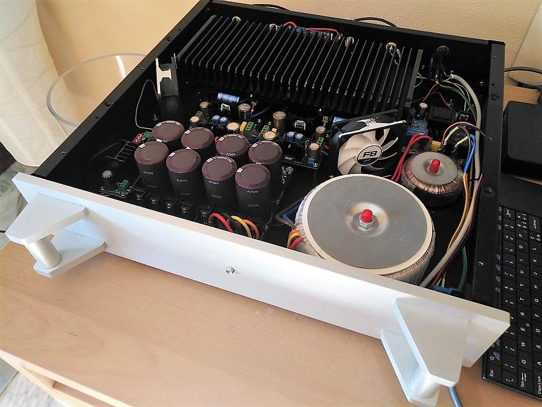
When playing music loud, the (aluminium) chassis that the transistors are bolted to gets warm right near the transistors (as one would expect) but it's stable. My chassis is also fully enclosed - no vents apart from a couple of holes on the rear panel.
There's no AC on the output.
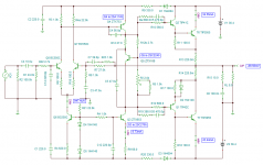
I have posted the revised schematic (27k -> 24k and 3k -> 2.7k changes) and simulation measurements with DC conditions. I also 'adjusted' the bias pot (in the simulation) to more accurately reflect my bias settings.
Incidentally - I checked the quiescent current yesterday, and both (+) and (-) legs are around 35mA, and remain stable there once the amp has settled.
It would seem my only issue is the DC offset, and at around +- 60mV, I'm really not sure if it's that much of an issue?
Interestingly, apart from the bias differences in AM3 / AM4 in the the simulation, it actually matches fairly closely with my 'real' amp.
Thanks to all for your suggestions.
Attachments
60 mV from OffSet for practical purposes is no problem for the speakers. However, if you could raise the supply voltage, even of the input differential and the VAS stage alone, you would see the OffSet collapse to less than 15/20 mV.
Measured last night, just for curiosity, on my NAP-140 clone, very similar to your H-140, the OffSet on the left channel is equal to 6 mVdc and on the right channel is equal to 11 mVdc.
Although in my case, at the time, I paired the two pairs of BC550s for HFE (given their derisory cost) with a selection made on 50 transistors.
Although in my case, at the time, I paired the two pairs of BC550s for HFE (given their derisory cost) with a selection made on 50 transistors.
Last edited:
<snip>...on my NAP-140 clone<snip>
Which boards do you have?
I see that there are several different types on Ebay now.
The most common version seems to have heatsinks on the drivers, which lay flat on the board, with the 2SC2922 output transistors.
Attachments
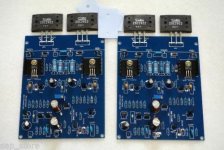
For some time now, it has become virtually impossible to find PCB versions of the NAIM NAP 140 clone similar to yours and mine.
To be exact, the one without the current protection net and with the TIP41/42 as drivers (that I have been replacing for years and in all my previous versions with the much more linear, refined and musical MJE15030/31 from ON Semiconductor) and the 2SC5200 as power transistors.
And even if I have already shown them in my previous posts, I send them again.
The two PCBs were photographed before I implemented the -/+ 40 Vdc stabilized power supply for the differential input stage and the VAS stage (V+2 / V-2), which in my version have the same transistors as your PCBs.
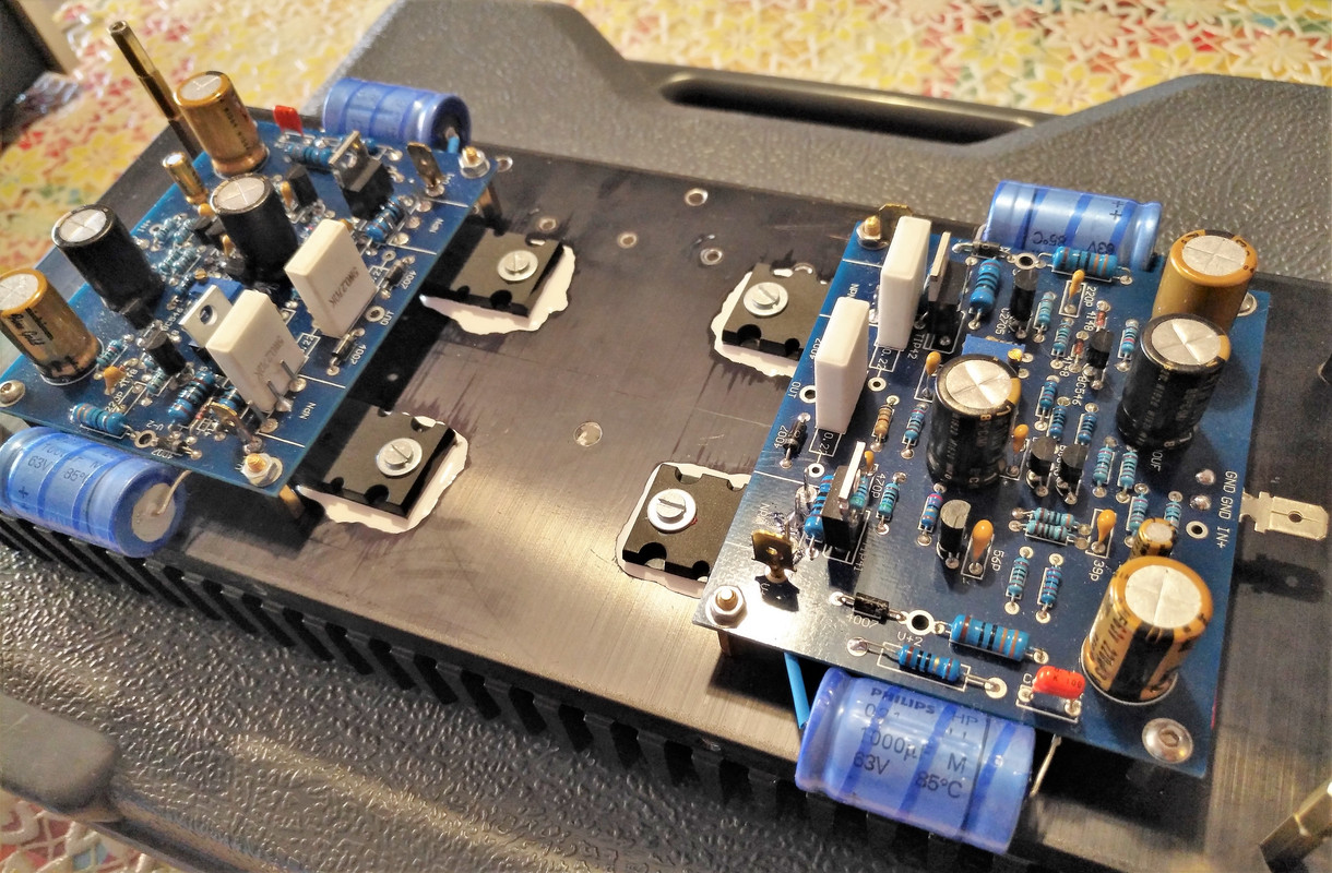
Last edited:
I found these boards on Aliexpress which look very similar, however they seem to have an additional pot, I presume for DC offset adjustment.
It shouldn't be too difficult to modify the board to the same circuit as ours though.
It shouldn't be too difficult to modify the board to the same circuit as ours though.
.Sorry but i will have to ask again....is it any diy pcb published for this amplifier?🙂
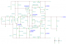
The following is the diagram that was normally sent with the H140 boards.
.
But far beyond this, a real mine of precious information is the following site that for subsequent upgrades has allowed me to get to my latest release of the clone NAP140 with an extraordinary musicality and able to drive with absolute authority any type of speaker passed from my stay between Thiel, Sonus Faber and Magnepan: Mods and upgrades
.I found these boards on Aliexpress which look very similar, however they seem to have an additional pot, I presume for DC offset adjustment.
It shouldn't be too difficult to modify the board to the same circuit as ours though.
Even if you can not understand the detail and type of transistors, it is very interesting to see the VBE multiplier that with the flat that is possible on the heatsink win at the power amps, although I fear overcompensation.
.
The suggestion to push the BIAS regulation to 150/200 mV is absolutely to be discarded.
.
Over 10/15 mV the trend of the Harmonic Distortion THD, in this circuit design no longer improves even a comma and exposes all the electronics to an unjustified thermal stress.
.
And I personally recommend any value between 7.0 and 9.5 mV.
Last edited:
@audio_tony
In your sim try changing R3 to 1.3k and see what the offset does.
Yeah, I'm with you too. It is an attempt that should be tried.
@audio_tony
In your sim try changing R3 to 1.3k and see what the offset does.
Yeah, I'm with you too. It is an attempt that should be tried.
Yes, that brings the offset to -7.97mV - perfect.
Attachments
- Home
- Amplifiers
- Solid State
- NAP-140 Clone Amp Kit on eBay