Thats very nice looking assembly work but I can assure you, that with the IPS power separated from the main power rails and with low Cob VAS transistors, it will sound nothing like a Naim clone. However, if this design is to your preference, then enjoy - it will be much closer to mainstream audio sound but possibly better quality if you are adjusting the values of passive components appropriately for the sweet spot of bias etc that is better suited to your substitute transistors.
One suggestion though - lose the craptanium TIP41/42 drivers. MJE243/253 are not really necessary with power transistors like 2SC5200/A1943 but they are more linear with better gain over a wider range of operating conditions such as sounding better over the full volume range which, as I found with many different Naim clones, was quite narrow and best with the volume quite low. Try the MJE types using genuine, not Ebay sourced parts. They are available in most major cities and by post from authorized European distributors. There are other, more suitable audio driver types from On Semi, Toshiba etc too so there are many, good quality options for you.
Thank you, Ian, for the nice words of appreciation.
It is confirmed, this is now the fifth release of the NAIM clone that I realize and after the first two, it is now several years that I have abandoned the original scheme consisting of protective net, fully linear power supply and the original ZTX transistors of the VAS stage.
Today's is actually an amplifier with a very different sound and that of the original NAIM only retains the particular talent for musical timing and the performance of a bass particularly fast, extended and articulated.
Clearly and always of course IMHO, what after years of attempts, modifications, refinements now sounds in my living room with an extraordinary musical nuance and a magnificent mix of timbre and sound-stage would not change with anything else.
As for the driver transistors, I unfortunately posted by mistake an old scheme because for 6 / 7 years now, I have definitely abandoned the TIP 41/42 for the MJE ON (personally after some tests I preferred MJE15030/MJE15031 to MJE243/MJE253) as actually in terms of delicate "breath" and refined detail of the mid and high, are at least two palms above.
And I have no difficulty in admitting that if today I have an amplifier that in my audio setup sounds like no other commercial amp purchased and tested in over 40 years of passion, I owe it also thanks to the important points of reflection that your posts and those of a few other friends of the forum, have been able to offer over time.
Thanks.
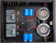
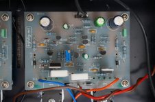
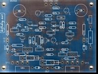
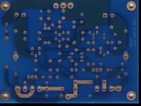
I just checked my boards (10 years on and still incomplete!!!) and they do indeed have places for caps - just not those caps... They are caps for the driver stages (c1 and c2 in the image - not yet fitted!)
Well, 11 years!! after I (partially) assembled these modules, I finally completed them and mounted them into a case with power supplies.
So far, I am quite impressed with the sound.
Transformers are from a Cambridge Audio 340A each with 2x 10000uF caps.
The PSU voltages are -+ 31vDC
They remained in my unfinished box for so long, because I was put off completing them after having read many stories of people not getting them to work properly, transistors marked the wrong way etc. However, after fitting the 220uF caps and power transistors to my boards, they just worked, so I need not have worried!
.
.
.
Attachments
Member
Joined 2009
Paid Member
Well, 11 years!! after I (partially) assembled these modules, I finally completed them and mounted them into a case with power supplies.
So far, I am quite impressed with the sound.
Transformers are from a Cambridge Audio 340A each with 2x 10000uF caps.
The PSU voltages are -+ 31vDC
They remained in my unfinished box for so long, because I was put off completing them after having read many stories of people not getting them to work properly, transistors marked the wrong way etc. However, after fitting the 220uF caps and power transistors to my boards, they just worked, so I need not have worried!
.
.
.
🙂🙂
.
Congratulations!

.
I have no difficulty in believing you when you talk about a good sound.
.
That exact PCB version, ten years ago, is exactly what after another couple of attempts with NAP 140 clone boards (with the historical ZTX transistors of the VAS stage and an overwhelming current protection) made me fall in love with this circuit design that I have never abandoned, preferring it also to commercial amplifiers costing 9/10 thousand Euros.
.
One question: by supplying it with a voltage of +/- 31 Volts, what OffSet Continuous Voltage do you measure on the speaker connectors?
.
@Bigun
@ultima legione
Thanks for the comments!
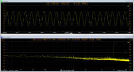
This afternoon I did some further measurements.
My PSU rails are actually +- 36.4vDC
DC offset: L channel: 100mV, Right channel: 91mV (these are probably on the high side.)
THD @1kHz 40W 8ohms = 0.0605%
THD @10kHz 40W 8 ohms = 0.0674%
I have attached THD spectrums.
Frequency response is flat beyond 20kHz at full power.
The channels in the spectrums are identical, because I was measuring a single channel only, but mono into both inputs on my sound card buffer.
I have not measured the other channel as yet, although expect it to be much the same.
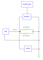
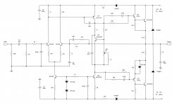
My measuring technique is AMP into dummy load (8 ohm resistor) and I take a tap of that via two 0.47ohm resistors (see attached schematic).
I think a better way to measure is to use a potential divider across the 8ohm load - but I read about the technique I'm using on the internet somewhere...
.
.
@ultima legione
Thanks for the comments!
This afternoon I did some further measurements.
My PSU rails are actually +- 36.4vDC
DC offset: L channel: 100mV, Right channel: 91mV (these are probably on the high side.)
THD @1kHz 40W 8ohms = 0.0605%
THD @10kHz 40W 8 ohms = 0.0674%
I have attached THD spectrums.
Frequency response is flat beyond 20kHz at full power.
The channels in the spectrums are identical, because I was measuring a single channel only, but mono into both inputs on my sound card buffer.
I have not measured the other channel as yet, although expect it to be much the same.
My measuring technique is AMP into dummy load (8 ohm resistor) and I take a tap of that via two 0.47ohm resistors (see attached schematic).
I think a better way to measure is to use a potential divider across the 8ohm load - but I read about the technique I'm using on the internet somewhere...
.
.
Attachments
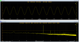
Beyond that, the spectral analysis at 1 KHz and 10 KHz seems to me much more than good and fully satisfies the already known and great performances of this circuit design in terms of Harmonic Distortion.
.
I confirm that the OffSet Voltage is certainly high for this type of amplifier.
.
When mounting the two transistors of the differential input circuit, did you respect the recommendation to install the one with the highest HFE (at least 10/15%), on the side of the signal input?
.
It is fundamental for a low OffSet and consider that on my amplifier they are at about 8/10 mV on both channels (therefore about one order of magnitude less than the 90/100 mV of your case) with a supply voltage of +/- 42 Vdc.
.
The output OffSet voltage tends to decrease anyway, with the increase of the dual supply voltage.
.
I confirm that the OffSet Voltage is certainly high for this type of amplifier.
.
When mounting the two transistors of the differential input circuit, did you respect the recommendation to install the one with the highest HFE (at least 10/15%), on the side of the signal input?
.
I didn't check the HFE, I had no idea I needed to do this. The instruction sheet I received with the kit consisted of a parts list, and some 'instructions' in Chinese.
I shall check that out, thanks.
In fact, it is unthinkable to find the various suggestions that gravitate around this historic audio project in the leaflet sent with the cards, but among the many tweaks is certainly one of the most important for the proper functioning of the amplifier.
.
To match the two pairs of BC550 of the input differential (one for the right channel and one for the left channel) with similar HFE values and with a 20% difference between those of the same channel, I even bought 4 or 5 tens of them.
.
Another important suggestion: contrary to the deceptive aspect of the PCB, it seems to me to remember that even in the case of your board, the BC550 that looks at the input signal is not the first one on the left but the opposite one.
.
Check carefully the circuit otherwise you risk to mount them just the opposite way.
.
To match the two pairs of BC550 of the input differential (one for the right channel and one for the left channel) with similar HFE values and with a 20% difference between those of the same channel, I even bought 4 or 5 tens of them.
.
Another important suggestion: contrary to the deceptive aspect of the PCB, it seems to me to remember that even in the case of your board, the BC550 that looks at the input signal is not the first one on the left but the opposite one.
.
Check carefully the circuit otherwise you risk to mount them just the opposite way.
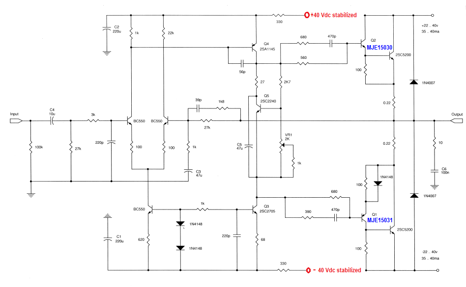
It doesn't help that the resistance to ground on the inverting input is 27k and the non-inverting is 30k, nor the 100 ohm emitter resistors that lower the transconductance, nor the use of different transistors than the original design.
With all these problems I wouldn't bother trying to hand-pick BC550s. Instead, adjust the 620 ohm current source resistor until your output offset is within 20mV.
With all these problems I wouldn't bother trying to hand-pick BC550s. Instead, adjust the 620 ohm current source resistor until your output offset is within 20mV.
Well, 11 years!! after I (partially) assembled these modules, I finally completed them and mounted them into a case with power supplies.
So far, I am quite impressed with the sound.
Transformers are from a Cambridge Audio 340A each with 2x 10000uF caps.
The PSU voltages are -+ 31vDC
They remained in my unfinished box for so long, because I was put off completing them after having read many stories of people not getting them to work properly, transistors marked the wrong way etc. However, after fitting the 220uF caps and power transistors to my boards, they just worked, so I need not have worried!
.
.
.
Since you have room in your cabinet to work quietly, I would like to suggest some modifications to this circuit, which can significantly improve the sound:
a) take the negative of the two speaker terminals directly from the central ground and eliminate the original one on the board output,
b) buy 4 quality 680/1000 uF/63V axial electrolytic capacitors (Philips/Vishay) and install them directly on the two boards with the terminals (positive and negative depending on the case) soldered directly on the 2SC5200 power transistors,
c) Replace the two original 220 uF capacitors of the boards with quality NICHIKON MUSE Series capacitors and solder in parallel on their leads, under the board, two 100 nF WIMA polypropylene capacitors,
d) installs in parallel to the two 10.000 uF capacitors of each power rail (positive and negative) two 150 KOHM resistors,
e) when you can foresee the installation of two stabilized power supply modules of +/- 40 Vdc, disconnect the 4007 diodes present on each power supply rail and use the -V2/+V2 predispositions to supply the differential input stage and the VAS stage.
It doesn't help that the resistance to ground on the inverting input is 27k and the non-inverting is 30k, nor the 100 ohm emitter resistors that lower the transconductance, nor the use of different transistors than the original design.
With all these problems I wouldn't bother trying to hand-pick BC550s. Instead, adjust the 620 ohm current source resistor until your output offset is within 20mV.
+1
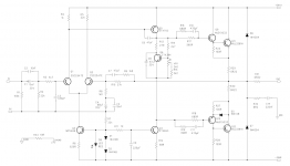
I note that the circuit published by Neil McBride has an LED in parallel with D1 and D2 (1n4148) which would also change the bias current for the input pair.
I wonder why this has been left out in the clone?
Additionally, there is also a compensation network across the main feedback resistor that isn't in the clone.
Also - the input resistor in the original is 22k with a 4k7 series resistor, which balances out the 27k feedback resistor.
Might it be worth changing my boards to match these values?
EDIT: I've just realised my clone is based on the Avondale NCC200
.
Attachments
Last edited:
It doesn't help that the resistance to ground on the inverting input is 27k and the non-inverting is 30k, nor the 100 ohm emitter resistors that lower the transconductance, nor the use of different transistors than the original design.
With all these problems I wouldn't bother trying to hand-pick BC550s. Instead, adjust the 620 ohm current source resistor until your output offset is within 20mV.
I think ultima_legione has done the tweaking by ears? If so, you can't say that those you mentioned were 'problems'.
(1) About unbalanced differential amp. I found that balancing the amp for better common mode performance is not the critical objective in an LTP.
(2) About the 100R emitter degeneration. Indeed, it makes transconductance suffers but it has it's own objective. I will usually try to avoid it but if I can't achieve certain objective other than using the emitter degeneration then may be I'll do it (but usually I'm more resourceful and skillful than that 😀). I think one of the Naim used the emitter degeneration resistors.
(3) Use of different transistors than the original will make it a different amp. We cannot use different VAS transistor and keep everything else the same. That will be wrong. If the VAS transistor is changed, expect more changes with other parts. If this sounds good (according to UL) compared to other expensive designs then, why it should be wrong? Any measurements here, UL?
(4) I will not rely on the 620R ccs resistor to lower the output offset. It can affect other things which is more important than just having high DC offset. Using high hfe part at the input side does make more sense.
ADD: I couldn't figure out which schematic was referred to by Traderbam.
In simulation, changing the 620R to 560R reduces the offset from 77mV to 50mV, and nothing else seems to change, apart from a (very) small reduction in simulated THD.
So I might just try this as a first step.
So I might just try this as a first step.
It's the same board as in post #494
Thanks for the answer but i mean a pcb that i can etching at home. 😉
The other option is that Prasi is hearing.

Last edited:
I was referring to post 3941.ADD: I couldn't figure out which schematic was referred to by Traderbam.
YesAlso - the input resistor in the original is 22k with a 4k7 series resistor, which balances out the 27k feedback resistor.
Might it be worth changing my boards to match these values?
- Home
- Amplifiers
- Solid State
- NAP-140 Clone Amp Kit on eBay