Depending on the transistor power rating and the type of instrument you are measuring Hfe with, you probably can't avoid inconsistent results, especially if the transistor heats up under the test conditions. The Atmega 328 testers use very low current to test with but this is not always appropriate for transistors rated 0.5W or more. Consequently, measurements should be done quickly and consistently without handling, to minimise the effect of thermal drift. The tester readout also only shows results in a stepped series of low resolution values rather than a smooth progression like a DMM. Neither these testers or the transistor test sockets on multimeters are calibrated, so we can't expect much accuracy with them either.gent ebay h140 clone looking for some advice re input pair matching some post say shoud be the same and avondale say tr1 shoud be 10% more, i have got from mouser 100 divices bc546bta fairchid about 45 % hfe 286, 45% hfe 432 and 10% give strange reading and never the same so i tend to think bad bc546 or is this the norm
Suitable test jigs for matching signal level transistors have been posted here, in the parts forum and in many places and sites on the web. All you need is the usual piece of breadboard, a few parts, a DMM and a small power supply capable of at least 100 mA. In other words, learn to search topics for yourself with an engine that works, like Google. search "transistor matching jig"
Re: the closeness of match: I think its obvious that If its a Naim clone you're trying to build then you follow their recommendations and vice versa for for Avondale designs. The settings and transistor matches are for some particular sound quality and there is no right or wrong method, just the appropriate one for the design you choose to clone. If you are trying to replace MPSA06, it should be obvious that Hfe value of the BC546 or other substitute, should be in the datasheet range of the MPSA06. It is only used in general purpose applications here, so matching is not necessary.
Last edited:
Ian thx for the info. my main speakers 4 way with 6 amps in each mods to date are input bc 546 tr 4,6 ztx tr 5 2n5551 drivers mje15030,1 out put 2sc5200 all from mouser. input cap evox mmk 3.3 uf feed back vbe biasing evox mmk 47uf, however of set was not as bad is i rember 25 to 40 mv and thay did not sound right so next move oscon solid aly 47 uf vbe biasing, feed back Axial Tantalum wow night and day stuff need a bit of running 8 hrs the tants are only 50usd for 50 MilitaryGrade USSR 50x K53-4 ( 68uF 20% , 15V ) Axial Tantalum Capacitors Military Grade BOX USSR | eBay anps are 140 Classic NAIM CLONE AMP CLONE DIY KIT 70W Mono | eBay
some adivice ztx mmm run very warm not mesured as yet heat sink or not never seen a picture of naim amps with heat sinks on them ( note i do work with big vfd drives up to 1000kw its just like a big class d amp) and as the norm would not like see a divice running that hot if you look at the data sheet case temp derating max out 200deg c you can make your tea with that comments please
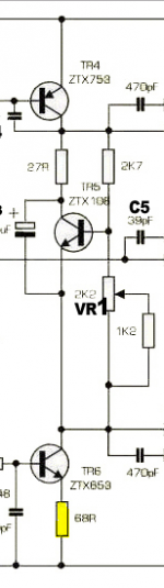
Calculate the current through the ZTX653/753 from the voltage drop across the 68R resistor. It should be only 6-8 mA and is not a problem if the correct series resistors and supply voltages are used. Note that 40V supplies are the maximum for the range of NAP designs and that in the original NAP140 amplifier, the supply rails were only +/- 34V. The attached schematic snip is from the generic NAP250 design used for the common Chinese clones.
E-line transistors such as these are small and consequently will run hotter than TO92 package transistors but as long as they don't "sizzle" with a moist finger on them, they should be fine. As an example of how tough these little monsters are, they were also used as driver transistors in the output stage of NAP90 and early NAIT models. Inside them is a medium power transistor chip, not a small signal type.
Capacitor types are always tinkered with by curious people for the possible sound effects. Effects though, are a matter of personal taste which can be weird indeed, perhaps also something that becomes boring or annoying over time. In any case, MMK types are metallized polyester film (like MKT and greencaps) which are compact but not the best quality for audio. Use electrolytic types where specified and don't mess with the values - use the correct value 10uF input cap. unless your amplifier is used only for HF applications. The 68uF feedback capacitor could be increased to 100uF or more without detriment though. Tantalum TAG capacitors are fine as long as you use new, fresh ones with adequate voltage rating to cope with likely fault conditions, accidental connections, over-voltage etc. and replace after perhaps only 10 years.
Attachments
Ian thank you for your comments re ztx and schematic and thay are the values i have fitted, my supply is +- 40v well +- 38v is the norm, your comment input cap i am going to give a try bc 125 10uf, more than once i wondered about the mmk, i do plan to mod the grounds as the boards i have only have one, the FB tants are 15v, all tested at 74uf +- 1 uf, the system has 40 hrs running and just sounds better even the wife commented what have done
Member
Joined 2009
Paid Member
Unless you are using Tantalum to be faithful to the original (?) another choice for the feedbac cap and the input cap are bipolar electrolytics. The MUSE series from Nichicon are excellent and I've used them in my best amps with superb results. This avoids the danger of over-voltage / revers-voltage conditions becoming a problem.
hi i have 25
i have tested e few
214 up to 275
I would avoid MPSA18. No info what is process 07. If it's Darlington that's very bad for this schematic.
Try standard transistors with beta 200-400.
Hi Ruwe, the MPSA18 question has come up in other threads too. Apparently they are just high Hfe, low noise BJTs, much like BC550c or 2N5089. I think these Caowei/ZeroZone NAP200 kits stick to old Motorola/On-Semi types because the pinout of MPS types is reversed to newer suitable types such as BC550C. That would cause confusion to many beginners as it did in the past when NAP140 Kits were supplied with a variety of cheap Japanese and Euro. type substitutes for the small-signal transistors.I would avoid MPSA18. No info what is process 07. If it's Darlington that's very bad for this schematic.
Try standard transistors with beta 200-400.
That's a large increase. It suggests that the parts you refitted to return to 1.5 mA, may now be wrong value, damaged or there is short or break in a trace that you haven't noticed. Check the collector resistor of Q1 which I assume is the same as TR1 on the Naim schematic(s) you find posted here.
Do you have the other channel complete for comparison?
Hi Ian and all the best for Happy New Year,
Tried to deal with dc out increase without success, the other channel is working perfectly and made some measurements. Also i replaced Q1,Q2 and Q3 keeping the rule of 10% hfe imbalance for Q1 and Q2 but dcoutput is the same.
Also i attached a schematic with voltages wich seems different to the working channel. In red between brakets are the voltages from "defective" channel.
I can adjust bias and is stable.
Restored the bias thru Q1 and Q2. Voltages on Q1, Q2, Q3 are the same in defective channel and working channel
My build is identical with schematic but i use MJE243/253 drivers and NJL0281power transistors
An externally hosted image should be here but it was not working when we last tested it.
free picture hosting
Last edited:
you have not attached "-" to the negative voltages.
To make your measured voltages clear, attach + & - so we can tell the difference between them.
To make your measured voltages clear, attach + & - so we can tell the difference between them.
Once the circuit is working properly, then you can look at output offset.
let's start with output offset exactly zero volts ref power ground (where the speaker will connect).
Current must flow from the output through the 27k to the base of TR2. If that base current is 2µA then the voltage across 27k will be 54mV
Since the current is flowing into the base, then the base must be sitting at -54mVdc relative to Power Ground.
The voltage across the BE of TR2 will be ~600mV. That places the emitter at ~-654mVdc
If you know the emitter current you can calculate the voltage at the bottom of the 100r degeneration resistor. (or you can measure it).
Now go back up the other side of the LTP.
Volts drop across the other degen resistor. Volts drop across BE of TR1 and you end up with the voltage at the base of TR1.
Now that base current must pass through 2k7 plus 24k to get back to Signal ground.
Signal ground is shown as commoned to power ground.
You can adjust the base voltages on the two LTP transistorts by adjusting the "resistances" the pass the quiescent base currents in those two transistors.
These base voltages are what determines the output offset of a properly working amplifier.
Since the 27k between the output and TR2 sets the amplifier gain, then you don't want to change that.
That leaves the 24k or the 2k7 (on the TR1 base) as your adjustment for output offset AFTER you have got the bad channel working properly.
You can measure and record all these Vdrops and compare channel to channel.
This applies to any BJT input LTP stage feeding a Power Amplifier.
It does not apply to jFET LTP where base current is virtually zero.
The jFET Vgs determines the output offset. And difference in Id of the two jFETs affects the Vgs difference and thus even with well matched jFETs the output offset can wander anywhere.
Last edited:
Ah, maybe you are right Andrew, thanks a lot for detailed explanation on how works this circuit.🙂 I will check again tonight. I think i ignored if the voltage was positive or negative as i measured in comparision with the working channnel. Also i did not used degeneration LTP 100r resistors. I replaced thos 100R with wire.
Last edited:
Omitting the degeneration resistors increases the gain of the input stage massively.
That is very likely to reduce the stability margins and worse, maybe turn it into an oscillator.
Sorry for all the typos in that post. I did read and re-read and edit where I saw it was necessary. But I missed some.
That is very likely to reduce the stability margins and worse, maybe turn it into an oscillator.
Sorry for all the typos in that post. I did read and re-read and edit where I saw it was necessary. But I missed some.
Last edited:
Andrew some advice please on the amps i have the 140 i have 27k and not 24k, 3k and not 2.7k should i change them
David
David
Hi,
I don't understand when your measurements are referred to. Anyway, looking at the base-emitter drops I would check T4, T5, T7 and adjacent components, especially the 47pF cap and the 68uF for shorts. It seems that current flows in opposite direction in the VAS, which is weird. Some of these transistors may be either shorted or the pin-out doesn't match with the board.
I don't understand when your measurements are referred to. Anyway, looking at the base-emitter drops I would check T4, T5, T7 and adjacent components, especially the 47pF cap and the 68uF for shorts. It seems that current flows in opposite direction in the VAS, which is weird. Some of these transistors may be either shorted or the pin-out doesn't match with the board.
Last edited:
Member
Joined 2009
Paid Member
Omitting the degeneration resistors increases the gain of the input stage massively.
That is very likely to reduce the stability margins and worse, maybe turn it into an oscillator.
High frequency stability aside, there is an interesting tradeoff that I haven't a clear picture on which way is best - the bass. With emitter degeneration the LTP is more linear over a wider differential signal swing. If this results in reduced distortion (esp. 2nd Harmonic) the bass tends to sound tighter. But if you leave the degeneration out the increased open loop gain results in a higher feedback factor and this reduces the differential signal at the LTP so you also win. I don't know which way is best for the NAP140, but the original design doesn't appear to use any degeneration and it seems to me that leaving it out is more faithful to the original sound (afterall, if you want a different sound you might be better off to start with another amplifier with fewer limitations). The higher feedback factor also benefits the PSRR of the amplifier.
Back to the stability. I don't really understand all the compensation elements. Cdom I get. Lead comp across the feedback resistor ? - usually this is a gateway for r.f. from speaker leads into the amplifier, especially when you have no output inductor in the basic design.
And what's with the R + C on the base stoppers to the drivers ?
Last edited:
Back to the stability. I don't really understand all the compensation elements. Cdom I get. Lead comp across the feedback resistor ? - usually this is a gateway for r.f. from speaker leads into the amplifier, especially when you have no output inductor in the basic design.
And what's with the R + C on the base stoppers to the drivers ?
I also tried to understand that some time ago.
IMO, the lead compensation in the feedback decreases the amp gain to something closer to 1, obviously before the phase shift is enough for instability to happen. As you said, the trade-off is the lower resistance in the feedback path and the RF path to the amp input.
The RC on the base stoppers adds some bandwidth, i.e. less resistance in the base combined with the base Miller capacitance will produce higher frequency low-pass filter. Some sort of phase reserve.
I think the designer needed to squeeze as much bandwidth as possible with acceptable high frequency phase shift from the driver transistors.
As we discussed here so many times, this circuit is tuned for the original components, layout etc., which makes it almost impossible to reproduce with DIY effort. I guess the right approach is to use frequency analyzer and fine tune it for best distortion/stability/bandwidth, testing stage by stage out of circuit, and finally the whole thing with the feedback in order to adjust the feedback RC. Haven't heard of any DIY enthusiast doing that.
It may turn into great sounding amp for very little money as Naim did more than 30 years ago... Or average and simple one for very little money, which is still OK for many DIY-ers.
Last edited:
Once the circuit is working properly, then you can look at output offset.
let's start with output offset exactly zero volts ref power ground (where the speaker will connect).
Current must flow from the output through the 27k to the base of TR2. If that base current is 2µA then the voltage across 27k will be 54mV
Since the current is flowing into the base, then the base must be sitting at -54mVdc relative to Power Ground.
The voltage across the BE of TR2 will be ~600mV. That places the emitter at ~-654mVdc
If you know the emitter current you can calculate the voltage at the bottom of the 100r degeneration resistor. (or you can measure it).
Now go back up the other side of the LTP.
Volts drop across the other degen resistor. Volts drop across BE of TR1 and you end up with the voltage at the base of TR1.
Now that base current must pass through 2k7 plus 24k to get back to Signal ground.
Signal ground is shown as commoned to power ground.
You can adjust the base voltages on the two LTP transistorts by adjusting the "resistances" the pass the quiescent base currents in those two transistors.
These base voltages are what determines the output offset of a properly working amplifier.
Since the 27k between the output and TR2 sets the amplifier gain, then you don't want to change that.
That leaves the 24k or the 2k7 (on the TR1 base) as your adjustment for output offset AFTER you have got the bad channel working properly.
You can measure and record all these Vdrops and compare channel to channel.
This applies to any BJT input LTP stage feeding a Power Amplifier.
It does not apply to jFET LTP where base current is virtually zero.
The jFET Vgs determines the output offset. And difference in Id of the two jFETs affects the Vgs difference and thus even with well matched jFETs the output offset can wander anywhere.
I started withAndrew some advice please on the amps i have the 140 i have 27k and not 24k, 3k and not 2.7k should i change them
David
"Once the circuit is working properly, then you can look at output offset."
Is your Naim clone working properly?
- Home
- Amplifiers
- Solid State
- NAP-140 Clone Amp Kit on eBay